SNOSAW2Q September 2006 – November 2015 LM5100A , LM5100B , LM5100C , LM5101A , LM5101B , LM5101C
PRODUCTION DATA.
- 1 Features
- 2 Applications
- 3 Description
- 4 Revision History
- 5 Device Comparison Table
- 6 Pin Configuration and Functions
- 7 Specifications
- 8 Detailed Description
- 9 Application and Implementation
- 10Power Supply Recommendations
- 11Layout
- 12Device and Documentation Support
- 13Mechanical, Packaging, and Orderable Information
9 Application and Implementation
NOTE
Information in the following applications sections is not part of the TI component specification, and TI does not warrant its accuracy or completeness. TI’s customers are responsible for determining suitability of components for their purposes. Customers should validate and test their design implementation to confirm system functionality.
9.1 Application Information
To affect fast switching of power devices and reduce associated switching power losses, a powerful gate driver is employed between the PWM output of controllers and the gates of the power semiconductor devices. Also, gate drivers are indispensable when it is impossible for the PWM controller to directly drive the gates of the switching devices. With the advent of digital power, this situation will be often encountered because the PWM signal from the digital controller is often a 3.3-V logic signal which cannot effectively turn on a power switch. Level shifting circuitry is needed to boost the 3.3-V signal to the gate-drive voltage (such as 12 V) in order to fully turn on the power device and minimize conduction losses. Traditional buffer drive circuits based on NPN/PNP bipolar transistors in totem-pole arrangement, being emitter follower configurations, prove inadequate with digital power because they lack level-shifting capability. Gate drivers effectively combine both the level-shifting and buffer-drive functions. Gate drivers also find other needs such as minimizing the effect of high-frequency switching noise by locating the high-current driver physically close to the power switch, driving gate-drive transformers and controlling floating power-device gates, reducing power dissipation and thermal stress in controllers by moving gate charge power losses from the controller into the driver.
The LM5100A/B/C and LM5101A/B/C are the high voltage gate drivers that are designed to drive both the high-side and low-side N-Channel MOSFETs in a half-bridge/full bridge configuration or in a synchronous buck circuit. The floating high side driver is capable of operating with supply voltages up to 100 V. This allows for N-Channel MOSFET control in half-bridge, full-bridge, push-pull, two switch forward and active clamp topologies. The outputs are independently controlled. Each channel is controlled by its respective input pins (HI and LI), allowing full and independent flexibility to control on and off state of the output.
9.2 Typical Application
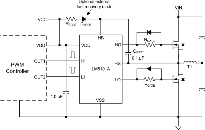 Figure 25. LM5101A Driving MOSFETs in Half-Bridge Configuration
9.2.1 Design Requirements
See Table 2 for the parameter and values.
Table 2. Operating Parameters
| PARAMETER | VALUE |
|---|---|
| Gate Driver | LM5101A |
| MOSFET | CSD18531Q5A |
| VDD | 10 V |
| Qgmax | 43 nC |
| Fsw | 100 kHz |
| Dmax | 95% |
| IHBS | 10 µA |
| VDH | 1.0 V |
| VHBR | 7.1 V |
| VHBH | 0.4 V |
9.2.2 Detailed Design Procedure
9.2.2.1 Select Bootstrap and VDD capacitor
The bootstrap capacitor must maintain the HB pin voltage above the UVLO voltage for the HB circuit in any circumstances during normal operation. Calculate the maximum allowable drop across the bootstrap capacitor with Equation 1.
where
- VDD = Supply voltage of the gate drive IC
- VDH = Bootstrap diode forward voltage drop
- VHBL = VHBR – VHBH = 6.7 V, HB falling threshold
The quiescent current of the bootstrap circuit is 10 µA, which is negligible compared to the Qgs of the MOSFET
(see Equation 2 and Equation 3).


In practice the value for the CBOOT capacitor should be greater than that calculated to allow for situations where the power stage may skip pulse due to load transients. It is recommended to place the bootstrap capacitor as close to the HB and HS pins as possible.
As a general rule the local VDD bypass capacitor should be 10 times greater than the value of CBOOT.
The bootstrap and bias capacitors should be ceramic types with X7R dielectric. The voltage rating should be twice that of the maximum VDD to allow for loss of capacitance once the devices have a DC bias voltage across them and to ensure long-term reliability of the devices.
9.2.2.2 Select External Bootstrap Diode and Resistor
The bootstrap capacitor is charged by the VDD through the internal bootstrap diode every cycle when low side MOSFET turns on. The charging of the capacitor involves high peak currents, and therefore transient power dissipation in the internal bootstrap diode may be significant and dependent on its forward voltage drop. Both the diode conduction losses and reverse recovery losses contribute to the total losses in the gate driver and need to be considered in the gate driver IC power dissipation.
For high frequency and high capacitive loads, it may be necessary to consider using an external bootstrap diode placed in parallel with internal bootstrap diode to reduce power dissipation of the driver. For the selection of external bootstrap diodes for LM510x device, please refer to the application note SNVA083.
Bootstrap resistor RBOOT is selected to reduce the inrush current in DBOOT and limit the ramp up slew rate of voltage of HB-HS. It is recommended that RBOOT is between 2 Ω and 10 Ω. For this design, a current limiting resistor of 2.2 Ω is selected to limit inrush current of bootstrap diode.

9.2.2.3 Select Gate driver Resistor
Resistor RGATE is sized to reduce ringing caused by parasitic inductances and capacitances and also to limit the current coming out of the gate driver. For this design 4.7-Ω resistors were selected for this design. Maximum HO and LO drive current are calculated by Equation 7 through Equation 10.


where
- IHOH = Maximum HO source current
- ILOH = Maximum LO source current
- IHOL = Maximum HO sink current
- ILOH = Maximum HO sink current
- VOH = High-Level output voltage drop across HB to HO or VDD to LO
- VOL = Low-Level output voltage drop across HO to HS or LO to GND
9.2.2.4 Estimate the Driver Power Losses
The total IC power dissipation is the sum of the gate driver losses and the bootstrap diode losses. The gate driver losses are related to the switching frequency (fsw), output load capacitance on LO and HO (CL), and supply voltage (VDD). The gate charge losses can be calculated by Equation 11.

There are some additional losses in the gate drivers due to the internal CMOS stages used to buffer the LO and HO outputs. The following plot shows the measured gate driver power dissipation versus frequency and load capacitance. At higher frequencies and load capacitance values, the power dissipation is dominated by the power losses driving the output loads and agrees well with Equation 11. Figure 26 can be used to approximate the power losses due to the gate drivers.
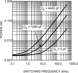 Figure 26. Gate Driver Power Dissipation (LO + HO)
VDD = 12 V, Neglecting Diode Losses
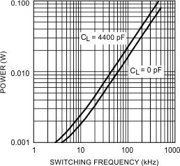
The internal bootstrap diode power loss is the sum of the forward bias power loss that occurs while charging the bootstrap capacitor and the reverse bias power loss that occurs during reverse recovery. Since each of these events happens once per cycle, the diode power loss is proportional to frequency. Larger capacitive loads require more energy to recharge the bootstrap capacitor resulting in more losses. Higher input voltages (VIN) to the half bridge result in higher reverse recovery losses. The following plot was generated based on calculation and lab measurements of the diode recovery time and current under several operating conditions. This can be useful for approximating the internal diode power dissipation. If the diode losses can be significant, an external diode placed in parallel with the internal bootstrap diode can be helpful to reduce power dissipation within the IC.
The total IC power dissipation can be estimated from the plots shown in Figure 26 and Figure 27 by summing the gate drive losses with the internal bootstrap diode losses for the intended application. For a given ambient temperature, the maximum allowable power loss of the IC can be defined as equation Equation 12.

where
- Ploss = The total power dissipation of the driver
- TJ = Junction temperature
- TA = Ambient temperature
- RθJA = Junction-to-ambient thermal resistance
The thermal metrics for the driver package is summarized in the Thermal Information table. For detailed information regarding the thermal information table, refer to the Application Note from Texas Instruments entitled Semiconductor and IC Package Thermal Metrics SPRA953.
9.2.3 Application Curves
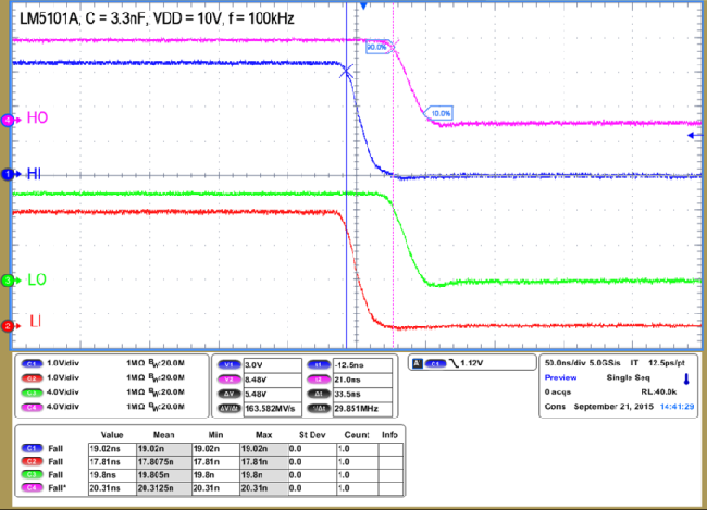 Figure 28. HI/LI to HO/LO Turnon Propagation Delay
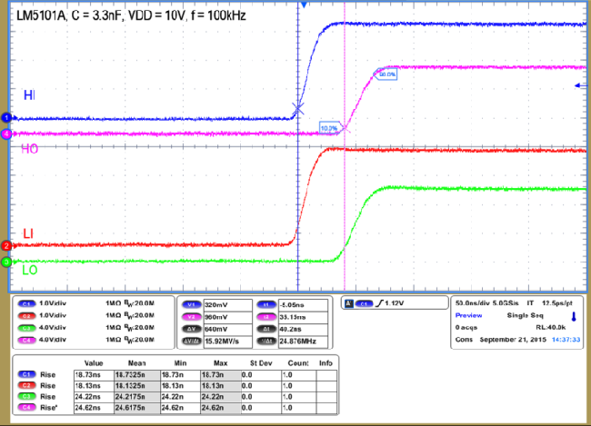 Figure 29. HI/LI to HO/LO Turnoff Propagation Delay
