SNVS412C April 2006 – September 2016 LM5109A
PRODUCTION DATA.
- 1 Features
- 2 Applications
- 3 Description
- 4 Revision History
- 5 Pin Configuration and Functions
- 6 Specifications
- 7 Detailed Description
- 8 Application and Implementation
- 9 Power Supply Recommendations
- 10Layout
- 11Device and Documentation Support
- 12Mechanical, Packaging, and Orderable Information
8 Application and Implementation
NOTE
Information in the following applications sections is not part of the TI component specification, and TI does not warrant its accuracy or completeness. TI’s customers are responsible for determining suitability of components for their purposes. Customers should validate and test their design implementation to confirm system functionality.
8.1 Application Information
To operate power MOSFETs at high switching frequencies and to reduce associated switching losses, a powerful gate driver is employed between the PWM output of controller and the gates of the power semiconductor devices. Also, gate drivers are indispensable when it is impossible for the PWM controller to directly drive the gates of the switching devices. With the advent of digital power, this situation is often encountered because the PWM signal from the digital controller is often a 3.3-V logic signal which cannot effectively turn on a power switch. Level shift circuit is needed to boost the 3.3-V signal to the gate-drive voltage (such as 12 V) to fully turn on the power device and minimize conduction losses. Traditional buffer drive circuits based on NPN and PNP bipolar transistors in totem-pole arrangement prove inadequate with digital power because they lack level-shifting capability. Gate drivers effectively combine both the level-shifting and buffer-drive functions. Gate drivers also find other needs such as minimizing the effect of high-frequency switching noise (by placing the high-current driver IC physically close to the power switch), driving gate-drive transformers and controlling floating power-device gates, reducing power dissipation and thermal stress in controllers by moving gate charge power losses from the controller into the driver.
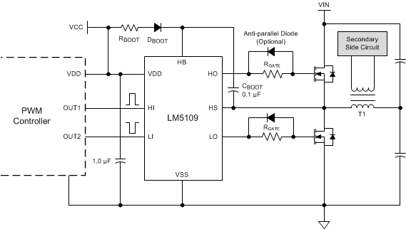
The LM5109A is the high-voltage gate drivers designed to drive both the high-side and low-side N-channel MOSFETs in a half-bridge configuration, full-bridge configuration, or in a synchronous buck circuit. The floating high-side driver is capable of operating with supply voltages up to 90 V. This allows for N-channel MOSFETs control in half-bridge, full-bridge, push-pull, two-switch forward and active clamp topologies. The outputs are independently controlled. Each channel is controlled by its respective input pins (HI and LI), allowing full and independent flexibility to control ON and OFF-time of the output.
8.1.1 HS Transient Voltages Below Ground
The HS node will always be clamped by the body diode of the lower external FET. In some situations, board resistances and inductances can cause the HS node to transiently swing several volts below ground. The HS node can swing below ground provided:
- HS must always be at a lower potential than HO. Pulling HO more than –0.3V below HS can activate parasitic transistors resulting in excessive current flow from the HB supply, possibly resulting in damage to the IC. The same relationship is true with LO and VSS. If necessary, a Schottky diode can be placed externally between HO and HS or LO and GND to protect the IC from this type of transient. The diode must be placed as close to the IC pins as possible in order to be effective.
- HB to HS operating voltage should be 15V or less. Hence, if the HS pin transient voltage is –5V, VDD should be ideally limited to 10V to keep HB to HS below 15V.
- Low ESR bypass capacitors from HB to HS and from VDD to VSS are essential for proper operation. The capacitor should be located at the leads of the IC to minimize series inductance. The peak currents from LO and HO can be quite large. Any series inductances with the bypass capacitor will cause voltage ringing at the leads of the IC which must be avoided for reliable operation.
8.2 Typical Application
 Figure 14. LM5109A Driving MOSFETs in a Half-Bridge Converter
8.2.1 Design Requirements
Table 2 lists the design parameters of the LM5109A.
Table 2. Design Example
| PARAMETER | VALUE |
|---|---|
| Gate Driver | LM5109A |
| MOSFET | CSD19534KCS |
| VDD | 10 V |
| QG | 17 nC |
| fSW | 500 kHz |
8.2.2 Detailed Design Procedure
8.2.2.1 Select Bootstrap and VDD Capacitor
The bootstrap capacitor must maintain the VHB-HS voltage above the UVLO threshold for normal operation. Calculate the maximum allowable drop across the bootstrap capacitor with Equation 1.

where
- VDD = Supply voltage of the gate drive IC
- VDH = Bootstrap diode forward voltage drop
- VHBL = VHBRmax – VHBH, HB falling threshold
Then, the total charge needed per switching cycle is estimated by Equation 2.

where
- QG = Total MOSFET gate charge
- IHBS = HB to VSS Leakage current
- DMax = Converter maximum duty cycle
- IHB = HB Quiescent current
Therefore, the minimum CBoot must be:

In practice, the value of the CBoot capacitor must be greater than calculated to allow for situations where the power stage may skip pulse due to load transients. TI recommends having enough margins and place the bootstrap capacitor as close to the HB and HS pins as possible.
As a general rule the local VDD bypass capacitor must be 10 times greater than the value of CBoot, as shown in Equation 5.
The bootstrap and bias capacitors must be ceramic types with X7R dielectric. The voltage rating must be twice that of the maximum VDD considering capacitance tolerances once the devices have a DC bias voltage across them and to ensure long-term reliability.
8.2.2.2 Select External Bootstrap Diode and Its Series Resistor
The bootstrap capacitor is charged by the VDD through the external bootstrap diode every cycle when low-side MOSFET turns on. The charging of the capacitor involves high peak currents, and therefore transient power dissipation in the bootstrap diode may be significant and the conduction loss also depends on its forward voltage drop. Both the diode conduction losses and reverse recovery losses contribute to the total losses in the gate driver circuit.
For the selection of external bootstrap diodes, see AN-1317 Selection of External Bootstrap Diode for LM510X Devices (SNVSA083). Bootstrap resistor RBOOT is selected to reduce the inrush current in DBOOT and limit the ramp up slew rate of voltage of VHB-HS during each switching cycle, especially when HS pin have excessive negative transient voltage. RBOOT recommended value is between 2 Ω and 10 Ω depending on diode selection. A current limiting resistor of 2.2 Ω is selected to limit inrush current of bootstrap diode, and the estimated peak current on the DBoot is shown in Equation 6.

where
- VDH is the bootstrap diode forward voltage drop
8.2.2.3 Selecting External Gate Driver Resistor
The external gate driver resistor, RGATE, is sized to reduce ringing caused by parasitic inductances and capacitances and also to limit the current coming out of the gate driver.
Peak HO pullup current are calculated in Equation 7.

where
- IOHH = Peak pullup current
- VDH = Bootstrap diode forward voltage drop
- RHOH = Gate driver internal HO pullup resistance, provide by driver data sheet directly or estimated from the testing conditions, that is RHOH = VOHH / IHO
- RGate = External gate drive resistance
- RGFET_Int = MOSFET internal gate resistance, provided by transistor data sheet
Similarly, Peak HO pulldown current is shown in Equation 8.

where
- RHOL is the HO pulldown resistance
Peak LO pullup current is shown in Equation 9.

where
- RLOH is the LO pullup resistance
Peak LO pulldown current is shown in Equation 10.

where
- RLOL is the LO pulldown resistance
For some scenarios, if the applications require fast turnoff, an anti-paralleled diode on RGate could be used to bypass the external gate drive resistor and speed up turnoff transition.
8.2.2.4 Estimate the Driver Power Loss
The total driver IC power dissipation can be estimated through the following components.
- Static power losses, PQC, due to quiescent current – IDD and IHB
- Level-shifter losses, PIHBS, due high-side leakage current – IHBS
- D is the high-side switch duty cycle
- Dynamic losses, PQG1&2, due to the FETs gate charge – QG
- QG = Total FETs gate charge
- fSW = Switching frequency
- RGD_R = Average value of pullup and pulldown resistor
- RGate = External gate drive resistor
- RGFET_Int = Internal FETs gate resistor
- Level-shifter dynamic losses, PLS, during high-side switching due to required level-shifter charge on each switching cycle – QP
where

where
In this example, the estimated gate driver loss in LM5109A is shown in Equation 15.

For a given ambient temperature, the maximum allowable power loss of the IC can be defined as shown in Equation 16.

where
- PLM5109B = The total power dissipation of the driver
- TJ = Junction temperature
- TA = Ambient temperature
- RθJA = Junction-to-ambient thermal resistance
The thermal metrics for the driver package is summarized in the Thermal Information table of the data sheet. For detailed information regarding the thermal information table, please refer to the Semiconductor and IC Package Thermal Metrics (SPRA953).
8.2.3 Application Curves
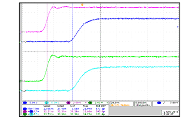
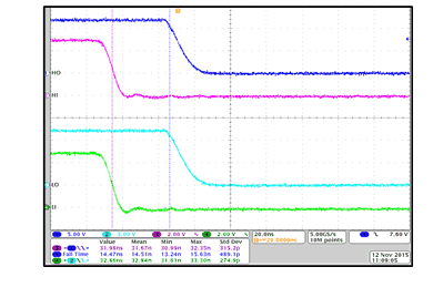
Figure 15 and Figure 16 shows the rising and falling time as well as turnon and turnoff propagation delay testing waveform in room temperature, and waveform measurement data (see the bottom part of the waveform). Each channel (HI, LI, HO, and LO) is labeled and displayed on the left hand of the waveforms.
The testing condition: load capacitance is 1 nF, VDD = 12 V, fSW = 500 kHz.
HI and LI share one same input from function generator, therefore, besides the propagation delay and rising and falling time, the difference of the propagation delay between HO and LO gives the propagation delay matching data.

| CL = 1 nF | VDD = 12 V | fSW = 500 kHz |

| CL = 1 nF | VDD = 12 V | fSW = 500 kHz |