SNVS412C April 2006 – September 2016 LM5109A
PRODUCTION DATA.
- 1 Features
- 2 Applications
- 3 Description
- 4 Revision History
- 5 Pin Configuration and Functions
- 6 Specifications
- 7 Detailed Description
- 8 Application and Implementation
- 9 Power Supply Recommendations
- 10Layout
- 11Device and Documentation Support
- 12Mechanical, Packaging, and Orderable Information
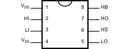
5 Pin Configuration and Functions
D Package
8-Pin SOIC
Top View

NGT Package
8-Pin WSON
Top View

Pin Functions
| Pin # | NAME | DESCRIPTION | APPLICATION INFORMATION | |
|---|---|---|---|---|
| SOIC | WSON(1) | |||
| 1 | 1 | VDD | Positive gate drive supply | Locally decouple to VSS using low ESR/ESL capacitor located as close to IC as possible. |
| 2 | 2 | HI | High side control input | The HI input is compatible with TTL input thresholds. Unused HI input should be tied to ground and not left open |
| 3 | 3 | LI | Low side control input | The LI input is compatible with TTL input thresholds. Unused LI input should be tied to ground and not left open. |
| 4 | 4 | VSS | Ground reference | All signals are referenced to this ground. |
| 5 | 5 | LO | Low side gate driver output | Connect to the gate of the low-side N- MOS device. |
| 6 | 6 | HS | High side source connection | Connect to the negative terminal of the bootstrap capacitor and to the source of the high-side N-MOS device. |
| 7 | 7 | HO | High side gate driver output | Connect to the gate of the high-side N-MOS device. |
| 8 | 8 | HB | High side gate driver positive supply rail | Connect the positive terminal of the bootstrap capacitor to HB and the negative terminal of the bootstrap capacitor to HS. The bootstrap capacitor should be placed as close to IC as possible. |
(1) For WSON package it is recommended that the exposed pad on the bottom of the package be soldered to ground plane on the PCB and the ground plane should extend out from underneath the package to improve heat dissipation.