SNVS255B May 2004 – September 2016 LM5110
PRODUCTION DATA.
- 1 Features
- 2 Applications
- 3 Description
- 4 Revision History
- 5 Device Options
- 6 Pin Configuration and Functions
- 7 Specifications
- 8 Detailed Description
- 9 Applications and Implementation
- 10Power Supply Recommendations
- 11Layout
- 12Device and Documentation Support
- 13Mechanical, Packaging, and Orderable Information
9 Applications and Implementation
NOTE
Information in the following applications sections is not part of the TI component specification, and TI does not warrant its accuracy or completeness. TI’s customers are responsible for determining suitability of components for their purposes. Customers should validate and test their design implementation to confirm system functionality.
9.1 Application Information
To operate fast switching of power MOSFETs at high switching frequencies and to reduce associated switching losses, a powerful gate driver is employed between the PWM output of controller and the gates of the power semiconductor devices. Also, gate drivers are indispensable when it is impossible for the PWM controller to directly drive the gates of the switching devices. With the advent of digital power, this situation is often encountered because the PWM signal from the digital controller is often a 3.3 V logic signal which cannot effectively turn on a power switch. Level shift circuit is needed to boost the 3.3 V signal to the gate-drive voltage (such as 12 V) in order to fully turn-on the power device and minimize conduction losses. Traditional buffer drive circuits based on NPN/PNP bipolar transistors in totem-pole arrangement prove inadequate with digital power because they lack level-shifting capability. Gate drivers effectively combine both the level-shifting and buffer-drive functions. Gate drivers also find other needs such as minimizing the effect of high-frequency switching noise (by placing the high-current driver IC physically close to the power switch), driving gate-drive transformers and controlling floating power-device gates, reducing power dissipation and thermal stress in controllers by moving gate charge power losses from the controller into the driver.
The LM5110 Dual Gate Driver replaces industry standard gate drivers with improved peak output current and efficiency. Each “compound” output driver stage includes MOS and bipolar transistors operating in parallel that together sink more than 5A peak from capacitive loads. Combining the unique characteristics of MOS and bipolar devices reduces drive current variation with voltage and temperature. Separate input and output ground pins provide Negative Drive Capability allowing the user to drive MOSFET gates with positive and negative VGS voltages.
9.2 Typical Application
 Figure 12. Simplified Power Converter Using Synchronous Rectifiers
 With Negative Off Gate Voltage
9.2.1 Design Requirements
To select proper device from LM5110 family, TI recommends first checking the appropriate logic for the outputs. LM5110-2 has dual inverting outputs; LM5110-1 has dual noninverting outputs; LM5110-3 have inverting channel A and noninverting channel B. Moreover, some design considerations must be evaluated first in order to make the most appropriate selection. Among these considerations are VCC, drive current, and power dissipation.
9.2.2 Detailed Design Procedure
9.2.2.1 Parallel Outputs
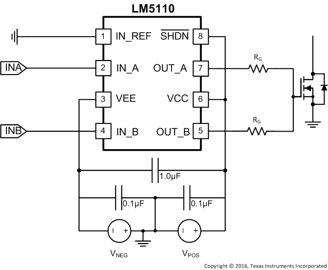
The A and B drivers may be combined into a single driver by connecting the INA/INB inputs together as close to the IC as possible, and the OUTA/OUTB outputs ties together if the external gate drive resistor is not used. In some cases where the external gate drive resistor is used, TI recommends that the resistor can be equally split in OUTA and OUTB respectively to reduce the parasitic inductance induce unbalance between two channels, as show in Figure 13.
 Figure 13. Parallel Operation of LM5110-1 and LM5110-2
Important consideration about paralleling two channels for LM5110 include: 1) IN_A and IN_B should be shorted in PCB layout as close to the device as possible, as well as for OUT_A and OUT_B, in which condition PCB layout parasitic mismatching between two channels could be minimized. 2) INA/B input slope signal should be fast enough to avoid mismatched VIH/VIL, td1/td2 between channel-A and channel-B. TI recommends having input signal slope faster than 20 V/µs.

