SNVS255B May 2004 – September 2016 LM5110
PRODUCTION DATA.
- 1 Features
- 2 Applications
- 3 Description
- 4 Revision History
- 5 Device Options
- 6 Pin Configuration and Functions
- 7 Specifications
- 8 Detailed Description
- 9 Applications and Implementation
- 10Power Supply Recommendations
- 11Layout
- 12Device and Documentation Support
- 13Mechanical, Packaging, and Orderable Information
11 Layout
11.1 Layout Guidelines
Attention must be given to board layout when using LM5110. Some important considerations include:
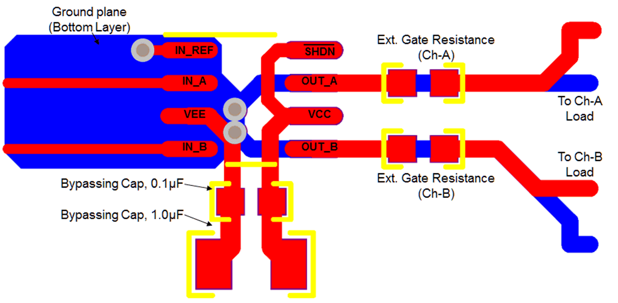
- A Low ESR/ESL capacitor must be connected close to the IC and between the VCC and VEE pins to support high peak currents being drawn from VCC during turn-on of the MOSFET.
- Proper grounding is crucial. The drivers need a very low impedance path for current return to ground avoiding inductive loops. The two paths for returning current to ground are a) between LM5110 IN-REF pin and the ground of the circuit that controls the driver inputs, b) between LM5110 VEE pin and the source of the power MOSFET being driven. All these paths should be as short as possible to reduce inductance and be as wide as possible to reduce resistance. All these ground paths should be kept distinctly separate to avoid coupling between the high current output paths and the logic signals that drive the LM5110. A good method is to dedicate one copper plane in a multi-layered PCB to provide a common ground surface.
- With the rise and fall times in the range of 10 ns to 30 ns, care is required to minimize the lengths of current carrying conductors to reduce their inductance and EMI from the high di/dt transients generated by the LM5110.
- The LM5110 SOIC footprint is compatible with other industry standard drivers. Simply connect IN_REF pin of the LM5110 to VEE (pin 1 to pin 3) to operate the LM5110 in a standard single supply configuration.
- If either channel is not being used, the respective input pin (IN_A or IN_B) should be connected to either IN_REF or VCC to avoid spurious output signals. If the shutdown feature is not used, the nSHDN pin should be connected to VCC to avoid erratic behavior that would result if system noise were coupled into a floating ’nSHDN’ pin.
11.2 Layout Example
 Figure 16. SOIC(8) Layout Example
11.3 Thermal Considerations
The primary goal of thermal management is to maintain the integrated circuit (IC) junction temperature (TJ) below a specified maximum operating temperature to ensure reliability. It is essential to estimate the maximum TJ of IC components in worst case operating conditions. The junction temperature is estimated based on the power dissipated in the IC and the junction to ambient thermal resistance θJA for the IC package in the application board and environment. The θJA is not a given constant for the package and depends on the printed circuit board design and the operating environment.
11.3.1 Drive Power Requirement Calculations in LM5110
The LM5110 dual low side MOSFET driver is capable of sourcing/sinking 3-A/5-A peak currents for short intervals to drive a MOSFET without exceeding package power dissipation limits. High peak currents are required to switch the MOSFET gate very quickly for operation at high frequencies.
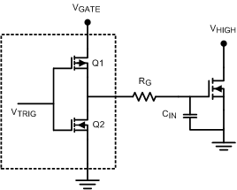
 Figure 17. LM5110 drives MOSFET with Driver Output Stage and MOSFET Gate-Source Capacitance
The schematic above shows a conceptual diagram of the LM5110 output and MOSFET load. Q1 and Q2 are the switches within the gate driver. RG is the gate resistance of the external MOSFET, and CIN is the equivalent gate capacitance of the MOSFET. The gate resistance Rg is usually very small and losses in it can be neglected. The equivalent gate capacitance is a difficult parameter to measure since it is the combination of CGS (gate to source capacitance) and CGD (gate to drain capacitance). Both of these MOSFET capacitances are not constants and vary with the gate and drain voltage. The better way of quantifying gate capacitance is the total gate charge QG in coloumbs. QG combines the charge required by CGS and CGD for a given gate drive voltage VGATE.
Assuming negligible gate resistance, the total power dissipated in the MOSFET driver due to gate charge is approximated by
where
- FSW = switching frequency of the MOSFET
As an example, consider the MOSFET MTD6N15 whose gate charge specified as 30 nC for VGATE = 12 V.
The power dissipation in the driver due to charging and discharging of MOSFET gate capacitances at switching frequency of 300 kHz and VGATE of 12 V is equal to
If both channels of the LM5110 are operating at equal frequency with equivalent loads, the total losses will be twice as this value which is 0.216 W.
In addition to the above gate charge power dissipation, - transient power is dissipated in the driver during output transitions. When either output of the LM5110 changes state, current will flow from VCC to VEE for a very brief interval of time through the output totem-pole N and P channel MOSFETs. The final component of power dissipation in the driver is the power associated with the quiescent bias current consumed by the driver input stage and undervoltage lockout sections.
Characterization of the LM5110 provides accurate estimates of the transient and quiescent power dissipation components. At 300-kHz switching frequency and 30-nC load used in the example, the transient power will be 8 mW. The 1-mA nominal quiescent current and 12-V VGATE supply produce a 12-mW typical quiescent power.
Therefore the total power dissipation
We know that the junction temperature is given by
Or the rise in temperature is given by
For SOIC-8 package θJA is estimated as 114°C/W see Thermal Information section.
Therefore TRISE is equal to
For WSON-10 package, the integrated circuit die is attached to leadframe die pad which is soldered directly to the printed circuit board. This substantially decreases the junction to ambient thermal resistance (θJA). θJA as low as 40°C/W is achievable with the WSON10 package. The resulting TRISE for the dual driver example above is thereby reduced to just 9.5°.
11.3.2 Continuous Current Rating of LM5110
The LM5110 can deliver pulsed source/sink currents of 3 A and 5 A to capacitive loads. In applications requiring continuous load current (resistive or inductive loads), package power dissipation, limits the LM5110 current capability far below the 5-A sink/3-A source capability. Rated continuous current can be estimated both when sourcing current to or sinking current from the load. For example when sinking, the maximum sink current can be calculated using Equation 7.

where
- RDS(on) is the on resistance of lower MOSFET in the output stage of LM5110.
Consider TJ(max) of 125°C and θJA of 114°C/W for an SO-8 package under the condition of natural convection and no air flow. If the ambient temperature (TA) is 60°C, and the RDS(on) of the LM5110 output at TJ(max) is 2.5 Ω, this equation yields ISINK(max) of 478 mA which is much smaller than 5-A peak pulsed currents.
Similarly, the maximum continuous source current can be calculated as

where
- VDIODE is the voltage drop across hybrid output stage which varies over temperature and can be assumed to be about 1.1 V at TJ(max) of 125°C
Assuming the same parameters as above, this equation yields ISOURCE(max) of 518 mA.