ZHCSTL7I February 2007 – November 2023 LM5116
PRODUCTION DATA
- 1
- 1 特性
- 2 应用
- 3 说明
- 4 Pin Configuration and Functions
- 5 Specifications
- 6 Detailed Description
-
7 Application and Implementation
- 7.1 Application Information
- 7.2
Typical Application
- 7.2.1 Design Requirements
- 7.2.2
Detailed Design Procedure
- 7.2.2.1 Custom Design with WEBENCH® Tools
- 7.2.2.2 Timing Resistor
- 7.2.2.3 Output Inductor
- 7.2.2.4 Current Sense Resistor
- 7.2.2.5 Ramp Capacitor
- 7.2.2.6 Output Capacitors
- 7.2.2.7 Input Capacitors
- 7.2.2.8 VCC Capacitor
- 7.2.2.9 Bootstrap Capacitor
- 7.2.2.10 Soft Start Capacitor
- 7.2.2.11 Output Voltage Divider
- 7.2.2.12 UVLO Divider
- 7.2.2.13 MOSFETs
- 7.2.2.14 MOSFET Snubber
- 7.2.2.15 Error Amplifier Compensation
- 7.2.2.16 Comprehensive Equations
- 7.2.3 Application Curves
- 7.3 Power Supply Recommendations
- 7.4 Layout
- 8 Device and Documentation Support
- 9 Revision History
- 10Mechanical, Packaging, and Orderable Information
6.3.2 Enable
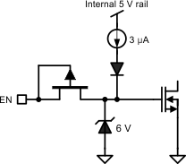
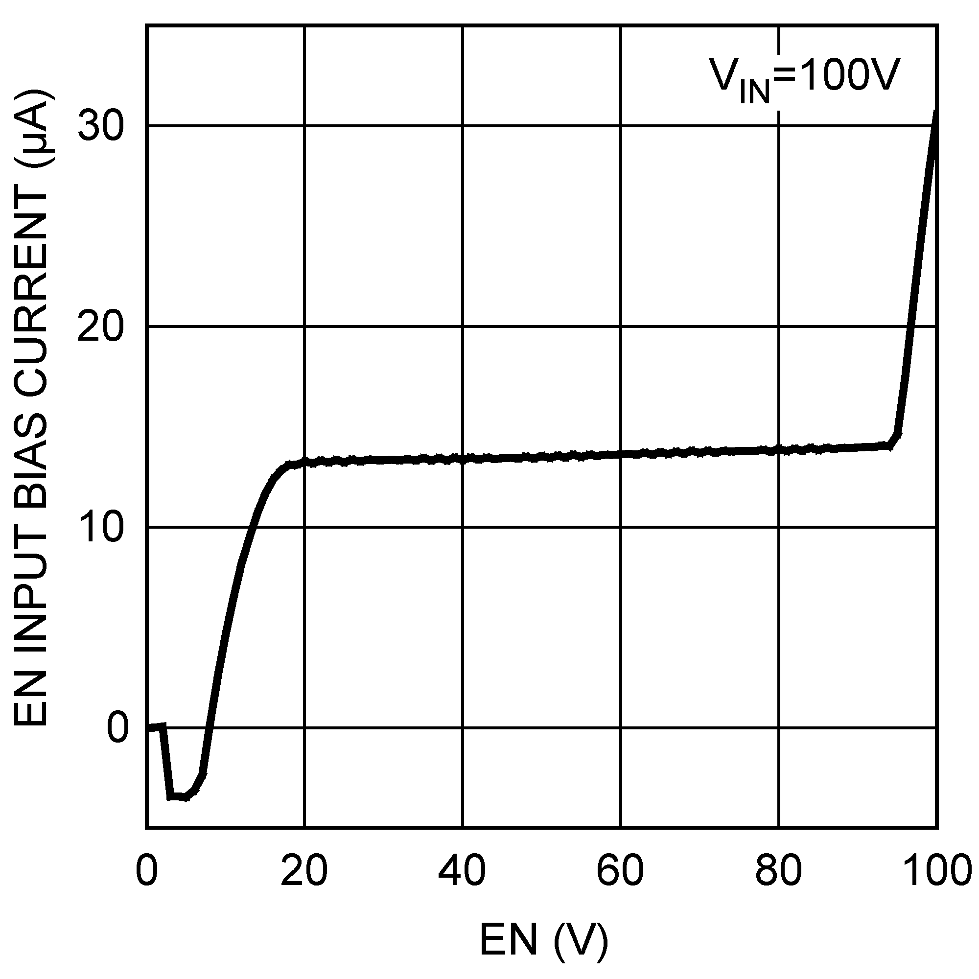
The LM5116 contains an enable function allowing a very low input current shutdown. If the enable pin is pulled below 0.5 V, the regulator enters shutdown, drawing less than 10 µA from the VIN pin. Raising the EN input above 3.3 V returns the regulator to normal operation. The maximum EN transition time for proper operation is one switching period. For example, the enable rise time must be less than 4 μs for 250-kHz operation.
A 1-MΩ pullup resistor to VIN can be used to interface with an open collector control signal. At low input voltage the pullup resistor can be reduced to 100 kΩ to speed up the EN transition time. The EN pin can be tied directly to VIN if this function is not needed. It must not be left floating. If low-power shutdown is not needed, the UVLO pin must be used as an on/off control.
 Figure 6-3 Enable Circuit
 Figure 6-4 EN Bias Current vs Voltage