ZHCS579F April 2011 – August 2015 LM5117 , LM5117-Q1
PRODUCTION DATA.
- 1 特性
- 2 应用
- 3 说明
- 4 修订历史记录
- 5 Pin Configuration and Functions
- 6 Specifications
-
7 Detailed Description
- 7.1 Overview
- 7.2 Functional Block Diagram
- 7.3
Feature Description
- 7.3.1 High Voltage Start-up Regulator and VCC Disable
- 7.3.2 UVLO
- 7.3.3 Oscillator and Sync Capability
- 7.3.4 Ramp Generator and Emulated Current Sense
- 7.3.5 Error Amplifier and PWM Comparator
- 7.3.6 Soft-Start
- 7.3.7 Cycle-by-Cycle Current Limit
- 7.3.8 Hiccup Mode Current Limiting
- 7.3.9 HO and LO Drivers
- 7.3.10 Current Monitor
- 7.3.11 Maximum Duty Cycle
- 7.3.12 Thermal Protection
- 7.4 Device Functional Modes
-
8 Application and Implementation
- 8.1 Application Information
- 8.2 Typical Applications
- 8.3
Detailed Design Procedure
- 8.3.1 Feedback Compensation
- 8.3.2 Sub-Harmonic Oscillation
- 8.3.3 Design Requirements
- 8.3.4 Timing Resistor RT
- 8.3.5 Output Inductor LO
- 8.3.6 Diode Emulation Function
- 8.3.7 Current Sense Resistor RS
- 8.3.8 Current Sense Filter RCS and CCS
- 8.3.9 Ramp Resistor RRAMP and Ramp Capacitor CRAMP
- 8.3.10 UVLO Divider RUV2, RUV1 and CFT
- 8.3.11 VCC Disable and External VCC Supply
- 8.3.12 Power Switches QH and QL
- 8.3.13 Snubber Components RSNB and CSNB
- 8.3.14 Bootstrap Capacitor CHB and Bootstrap Diode DHB
- 8.3.15 VCC Capacitor CVCC
- 8.3.16 Output Capacitor CO
- 8.3.17 Input Capacitor CIN
- 8.3.18 VIN Filter RVIN, CVIN
- 8.3.19 Soft-Start Capacitor CSS
- 8.3.20 Restart Capacitor CRES
- 8.3.21 Output Voltage Divider RFB2 and RFB1
- 8.3.22 Loop Compensation Components CCOMP, RCOMP and CHF
- 8.4 Application Curves
- 9 Power Supply Recommendations
- 10Layout
- 11器件和文档支持
- 12机械、封装和可订购信息
封装选项
机械数据 (封装 | 引脚)
散热焊盘机械数据 (封装 | 引脚)
订购信息
7 Detailed Description
7.1 Overview
The LM5117 high voltage switching controller features all of the functions necessary to implement an efficient high voltage buck regulator that operates over a very wide input voltage range. This easy to use controller integrates high-side and low-side NMOS drivers. The regulator control method is based upon peak current mode control utilizing an emulated current ramp. Peak current mode control provides inherent line feed-forward, cycle-by-cycle current limiting and ease of loop compensation. The use of an emulated control ramp reduces noise sensitivity of the PWM circuit, allowing reliable processing of the very small duty cycles necessary in high input voltage applications.
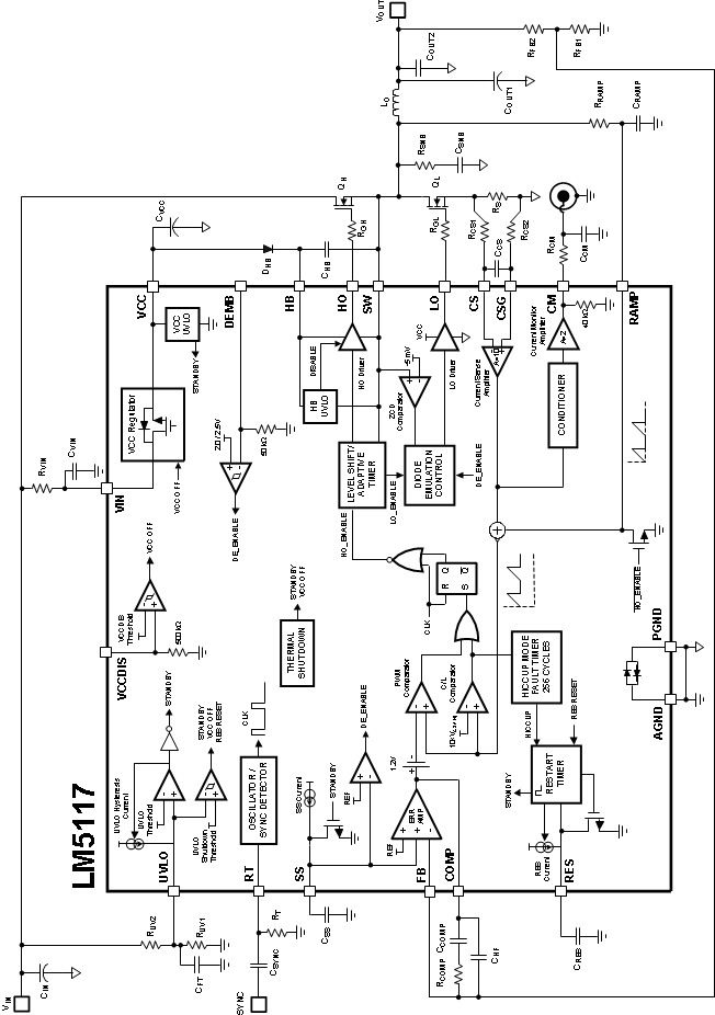
The switching frequency is user programmable up to 750 kHz. The RT pin allows the switching frequency to be programmed by a single resistor or synchronized to an external clock. Fault protection features include cycle-by-cycle and hiccup mode current limiting, thermal shutdown and remote shutdown capability by pulling down UVLO pin. The UVLO input enables the regulator when the input voltage reaches a user selected threshold and provides a very low quiescent shutdown current when pulled low. A unique analog telemetry feature provides averaged output current information, allowing various applications that need either a current monitor or current control. The functional block diagram and typical application circuit of the LM5117 are shown in Functional Block Diagram.
The device is available in a HTSSOP-20 (6.5 mm x 4.4 mm) package, as well as a WQFN-24 (4 mm × 4 mm) package which features an exposed pad to aid in thermal dissipation.
7.2 Functional Block Diagram
7.3 Feature Description
7.3.1 High Voltage Start-up Regulator and VCC Disable
The LM5117 contains an internal high voltage bias regulator that provides the VCC bias supply for the PWM controller and NMOS gate drivers. The VIN pin can be connected to an input voltage source as high as 65 V. The output of the VCC regulator is set to 7.6V. When the input voltage is below the VCC set-point level, the VCC output tracks the VIN with a small dropout voltage. The output of the VCC regulator is current limited at 30mA minimum.
Upon power-up, the regulator sources current into the capacitor connected to the VCC pin. The recommended capacitance range for the pin VCC is 0.47 µF to 10 µF. When the VCC pin voltage exceeds the VCC UV threshold and the UVLO pin is greater than UVLO threshold, the HO and LO drivers are enabled and a soft-start sequence begins. The HO and LO drivers remain enabled until either the VCC pin voltage falls below VCC UV threshold, the UVLO pin voltage falls below UVLO threshold, hiccup mode is activated or the die temperature exceeds the thermal shutdown threshold. Enabling/Disabling the IC by controlling UVLO is recommended in most of cases.
An output voltage derived bias supply can be applied to the VCC pin to reduce the controller power dissipation at higher input voltage. The VCCDIS input can be used to disable the internal VCC regulator when external biasing is supplied. The externally supplied bias should be coupled to the VCC pin through a diode, preferably a Schottky diode. If the VCCDIS pin voltage exceeds the VCCDIS threshold, the internal VCC regulator is disabled. VCCDIS has a 500-kΩ internal pull-down resistor to ground for normal operation with no external bias.
The VCC regulator series pass transistor includes a diode between VCC (Anode) and VIN (Cathode) that should not be forward biased in normal operation. If the voltage of the external bias supply is greater than the VIN pin voltage, an external blocking diode is required from the input power supply to the VIN pin to prevent the external bias supply from passing current to the input supply through VCC.
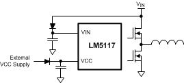 Figure 15. VIN Configuration for VVIN < VVCC
For VOUT between 6 V and 14.5 V, the output can be connected directly to VCC through a diode.
 Figure 16. External VCC Supply for 6 V < VOUT< 14.5 V
For VOUT < 6 V, a bias winding on the output inductor can be added to generate the external VCC supply voltage.
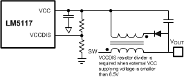 Figure 17. External VCC Supply for VOUT < 6 V
For 14.5 V <VOUT, the external supply voltage can be regulated by using a series Zener diode from the output to VCC.
 Figure 18. External VCC Supply for 14.5 V < VOUT
In high input voltage applications, extra care should be taken to ensure the VIN pin does not exceed the absolute maximum voltage rating of 75V. During line or load transients, voltage ringing on the VIN that exceeds the Absolute Maximum Rating can damage the IC. Both careful PC board layout and the use of quality bypass capacitors located close to the VIN and AGND pin are essential. Adding an R-C filter (RVIN, CVIN) on VIN is optional and helps to prevent faulty operation caused by poor PC board layout and high frequency switching noise injection. The recommended capacitance and resistance range are 0.1 µF to 10 µF and 1 Ω to 10 Ω.
7.3.2 UVLO
The LM5117 contains a dual level UVLO (under-voltage lockout) circuit. When the UVLO is less than 0.4 V, the LM5117 is in shutdown mode. The shutdown comparator provides 100 mV of hysteresis to avoid chatter during transitions. When the UVLO pin voltage is greater than 0.4 V but less than 1.25 V, the controller is in standby mode. In the standby mode, the VCC bias regulator is active but the HO and LO drivers are disabled and the SS pin is held low. This feature allows the UVLO pin to be used as a remote shutdown function by pulling the UVLO pin down below 0.4 V with an external open collector or open drain device. When the VCC pin exceeds its under-voltage lockout threshold and the UVLO pin voltage is greater than 1.25 V, the HO and LO drivers are enabled and normal operation begins.
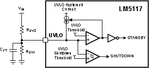 Figure 19. UVLO Configuration
The UVLO pin should not be left floating. An external UVLO set-point voltage divider from the VIN to AGND is used to set the minimum input operating voltage of the regulator. The divider must be designed such that the voltage at the UVLO pin is greater than 1.25 V and never exceeds 15 V when the input voltage is in the desired operating range. If necessary, the UVLO pin can be clamped with a Zener diode.
UVLO hysteresis is accomplished with an internal 20μA current source that is switched on or off into the impedance of the UVLO set-point divider. When the UVLO pin voltage exceeds the 1.25 V threshold, the current source is enabled to quickly raise the voltage at the UVLO pin. When the UVLO pin voltage falls below the 1.25 V threshold, the current source is disabled causing the voltage at the UVLO pin to quickly fall. The use of a CFT capacitor in parallel with RUV1 helps to minimize switching noise injection into UVLO pin, but it may slow down the falling speed of the UVLO pin when the 20 μA current source is disabled. The recommended range for CFT is 10 pF to 220 pF.
The values of RUV1 and RUV2 can be determined from the following equations:


where
- VHYS is the desired UVLO hysteresis and VIN(STARTUP) is the desired start-up voltage of the regulator during turn-on
7.3.3 Oscillator and Sync Capability
The LM5117 switching frequency is programmed by a single external resistor connected between the RT pin and the AGND pin. The resistor should be located very close to the device and connected directly to the RT and AGND pins. To set a desired switching frequency (ƒSW), the resistor value can be calculated from the following equation:

The RT pin can be used to synchronize the internal oscillator to an external clock. The internal oscillator can be synchronized by AC coupling a positive edge into the RT pin. The voltage at the RT pin is nominally 1.25 V and the voltage at the RT pin must exceed the RT Sync Positive Threshold to trip the internal synchronization pulse detector. A 5 V amplitude pulse signal coupled through a 100-pF capacitor is a good starting point. The frequency of the external synchronization pulse is recommended to be within ±10% of the frequency programmed by the RT resistor but will operate to +100/-40% of the programmed frequency. Care should be taken to guarantee that the RT pin voltage does not go below –0.3 V at the falling edge of the external pulse. This may limit the duty cycle of external synchronization pulse.
The RT resistor is always required, whether the oscillator is free running or externally synchronized.
7.3.4 Ramp Generator and Emulated Current Sense
The ramp signal used in the pulse width modulator for traditional current mode control is typically derived directly from the high-side switch current. This switch current corresponds to the positive slope portion of the inductor current. Using this signal for the PWM ramp simplifies the control loop transfer function to a single pole response and provides inherent input voltage feed-forward compensation.
The disadvantage of using the high-side switch current signal for PWM control is the large leading edge spike due to circuit parasitics that must be filtered or blanked. Minimum achievable pulse width is limited by the filtering, blanking time and propagation delay with a high-side current sensing scheme.
In the applications where the input voltage may be relatively large in comparison to the output voltage, controlling small pulse widths and duty cycles are necessary for regulation. The LM5117 utilizes a unique ramp generator which does not actually measure the high-side switch current but rather reconstructs the signal. Representing or emulating the inductor current provides a ramp signal to the PWM comparator that is free of leading edge spikes and measurement or filtering delays, while maintaining the advantages of traditional peak current mode control.
The current reconstruction is comprised of two elements: a sample-and-hold DC level and the emulated inductor current ramp as shown in Figure 20. The sample-and-hold DC level is derived from a measurement of the recirculating current flowing through the current sense resistor. The voltage across the sense resistor is sampled and held just prior to the onset of the next conduction interval of the high-side switch. The current sense amplifier with a gain of 10 and sample-and-hold circuit provide the DC level of the reconstructed current signal as shown in Figure 21.
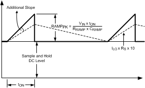 Figure 20. Composition of Emulated Current Sense Signal
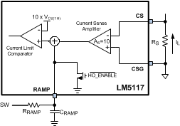 Figure 21. RAMP Generator and Current Limit Circuit
The positive slope inductor current ramp is emulated by CRAMP connected between RAMP and AGND and RRAMP connected between SW and RAMP. RRAMP should not be connected to VIN directly because the RAMP pin absolute maximum voltage rating could be exceeded under high input voltage conditions. CRAMP is discharged by an internal switch during the off-time and must be fully discharged during the minimum off-time. This limits the ramp capacitor to be less than 2 nF. A good quality, thermally stable ceramic capacitor is recommended for CRAMP.
The selection of RRAMP and CRAMP can be simplified by adopting a K factor, which is defined as:

where
- AS is the current sense amplifier gain which is normally 10
By choosing 1 as the K factor, the regulator removes any error after one switching cycle and the design procedure is simplified. See Application and Implementation for detailed information.
7.3.5 Error Amplifier and PWM Comparator
The internal high-gain error amplifier generates an error signal proportional to the difference between the FB pin voltage and the internal precision 0.8-V reference. The output of error amplifier is connected to the COMP pin allowing the user to provide Type 2 loop compensation components, RCOMP, CCOMP and optional CHF.
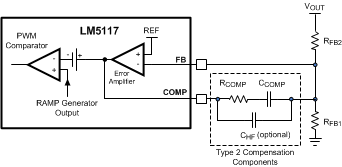 Figure 22. Feedback Configuration and PWM Comparator
RCOMP, CCOMP and CHF configure the error amplifier gain and phase characteristics to achieve a stable voltage loop gain. This network creates a pole at DC (FP1), a mid-band zero (FZ) for phase boost, and a high frequency pole (FP2). The recommended range of RCOMP is 2 kΩ to 40 kΩ. See Application and Implementation for detailed information.


The PWM comparator compares the emulated current sense signal from Ramp Generator to the voltage at the COMP pin through a 1.2-V internal voltage drop and terminates the present cycle when the emulated current sense signal is greater than VCOMP – 1.2 V.
7.3.6 Soft-Start
The soft-start feature allows the regulator to gradually reach the steady state operating point, thus reducing startup stresses and surges. The LM5117 regulates the FB pin to the SS pin voltage or the internal 0.8-V reference, whichever is lower. The internal 10-µA soft-start current source gradually increases the voltage on an external soft-start capacitor connected to the SS pin. This results in a gradual rise of the output voltage. Soft-start time (tss) can be calculated from the following equation:

The LM5117 can track the output of a master power supply during soft-start by connecting a voltage divider from the output of master power supply to the SS pin. At the beginning of the soft-start sequence, VSS should be allowed to go below 25 mV by the internal SS pull-down switch. During soft-start period, when SS pin voltage is less than 0.8V, the LM5117 forces diode emulation for startup into a pre-biased load. If the tracking feature is desired, connect the DEMB pin to GND or leave the pin floating.
7.3.7 Cycle-by-Cycle Current Limit
The LM5117 contains a current limit monitoring scheme to protect the regulator from possible over-current conditions as shown in Figure 21. If the emulated ramp signal exceeds 1.2 V, the present cycle is terminated. For the case where the switch current overshoots when the inductor is saturated or the output is shorted to ground, the sample-and-hold circuit detects the excess recirculating current before the high-side NMOS driver is turned on again. The high-side NMOS driver is disabled and will skip pulses until the current has decayed below the current limit threshold. This approach prevents current runaway conditions since the inductor current is forced to decay to a controlled level following any current overshoot.
Maximum peak inductor current can be calculated as:


where
- IPP represents inductor peak to peak ripple current in Figure 23, and is defined as:

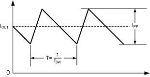 Figure 23. Inductor Current
During an output short condition, the worst case peak inductor current is limited to:

where
- tON(MIN) is the minimum HO on-time
In most cases, especially if the output voltage is relatively high, it is recommended that a soft-saturating inductor such as a powder core device is used. If a sharp-saturating inductor is used, the inductor saturation level must be above ILIM_PK. The temperatures of the NMOS devices, RS and inductor should be checked under this output short condition.
7.3.8 Hiccup Mode Current Limiting
To further protect the regulator during prolonged current limit conditions, LM5117 provides a hiccup mode current limit. An internal hiccup mode fault timer counts the PWM clock cycles during which cycle-by-cycle current limiting occurs. When the hiccup mode fault timer detects 256 consecutive cycles of current limiting, an internal restart timer forces the controller to enter a low power dissipation standby mode and starts sourcing 10 μA of current into the RES pin capacitor CRES. In this standby mode, HO and LO outputs are disabled and the soft-start capacitor CSS is discharged.
CRES is connected from RES pin to AGND and determines the time (tRES) in which the LM5117 remains in the standby before automatically restarting. When the RES pin voltage exceeds the 1.25-V RES threshold, RES capacitor is discharged and a soft-start sequence begins. tRES can be calculated from the following equation:

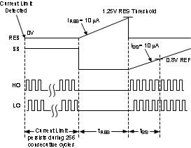 Figure 24. Hiccup Mode Current Limit Timing Diagram
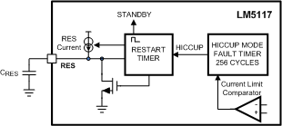 Figure 25. Hiccup Mode Current Limit Circuit
The RES pin can also be configured for latch-off mode current limiting or non-hiccup mode cycle-by-cycle current limiting. If the RES pin is tied to VCC or a voltage greater than the RES threshold at initial power-on, the restart timer is disabled and the regulator operates with non-hiccup mode cycle-by-cycle current limit. If the RES pin is tied to GND, the regulator enters into the standby mode after 256 consecutive cycles of current limiting and then never restarts until UVLO shutdown is cycled. The restart timer is configured during initial power-on when UVLO is above the UVLO threshold and VCC is above the VCC UV threshold.
 Figure 26. RES Configurations
7.3.9 HO and LO Drivers
The LM5117 contains high current NMOS drivers and an associated high-side level shifter to drive the external high-side NMOS device. This high-side gate driver works in conjunction with an external diode DHB, and bootstrap capacitor CHB. A 0.1-μF or larger ceramic capacitor, connected with short traces between the HB and SW pin, is recommended. During the off-time of the high-side NMOS driver, the SW pin voltage is approximately 0V and the CHB is charged from VCC through the DHB. When operating with a high PWM duty cycle, the high-side NMOS device is forced off each cycle for 320 ns to ensure that CHB is recharged.
The LO and HO outputs are controlled with an adaptive dead-time methodology which insures that both outputs are never enabled at the same time. When the controller commands HO to be enabled, the adaptive dead-time logic first disables LO and waits for the LO voltage to drop. HO is then enabled after a small delay (LO Fall to HO Rise Delay). Similarly, the LO turn-on is delayed until the HO voltage has discharged. LO is then enabled after a small delay (HO Fall to LO Rise Delay). This technique insures adequate dead-time for any size NMOS device, especially when VCC is supplied by a higher external voltage source. The adaptive dead-time circuitry monitors the voltages of HO and LO outputs and insures the dead-time between the HO and LO outputs. Adding a gate resister, RGH or RGL, may decrease the effective dead-time.
Care should be exercised in selecting an output NMOS device with the appropriate threshold voltage, especially if VCC is supplied by an external bias supply voltage below the VCC regulation level. During startup at low input voltages, the low-side NMOS device gate plateau voltage should be lower than the VCC under-voltage lockout threshold. Otherwise, there may be insufficient VCC voltage to completely enhance the NMOS device as the VCC under-voltage lockout is released during startup. If the high-side NMOS drive voltage is lower than the high-side NMOS device gate plateau voltage during startup, the regulator may not start or it may hang up momentarily in a high power dissipation state. This condition can be addressed by selecting an NMOS device with a lower threshold voltage. This situation can be avoided if the minimum input voltage programmed by the UVLO resistor is above the VCC regulation level.
7.3.10 Current Monitor
The LM5117 provides average output current information, enabling various applications requiring monitoring or control of the output current.
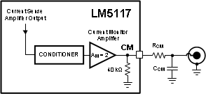 Figure 27. Current Monitor
The average of CM output can be calculated by:

The current monitor output is only valid in continuous conduction operation. The current monitor has a limited bandwidth of approximately one tenth of fSW. Adding an R-C filter, RCM and CCM, on the output of current monitor with the cut off frequency below one tenth of fSW is recommended to attenuate sampling noise.
7.3.11 Maximum Duty Cycle
When operating with a high PWM duty cycle, the high-side NMOS device is forced off each cycle for 320ns to ensure that CHB is recharged and to allow time to sample and hold the current in the low-side NMOS FET. This forced off-time limits the maximum duty cycle of the controller. When designing a regulator with high switching frequency and high duty cycle requirements, a check should be made of the required maximum duty cycle against the graph shown in Figure 28. The actual maximum duty cycle varies with the switching frequency as follows:
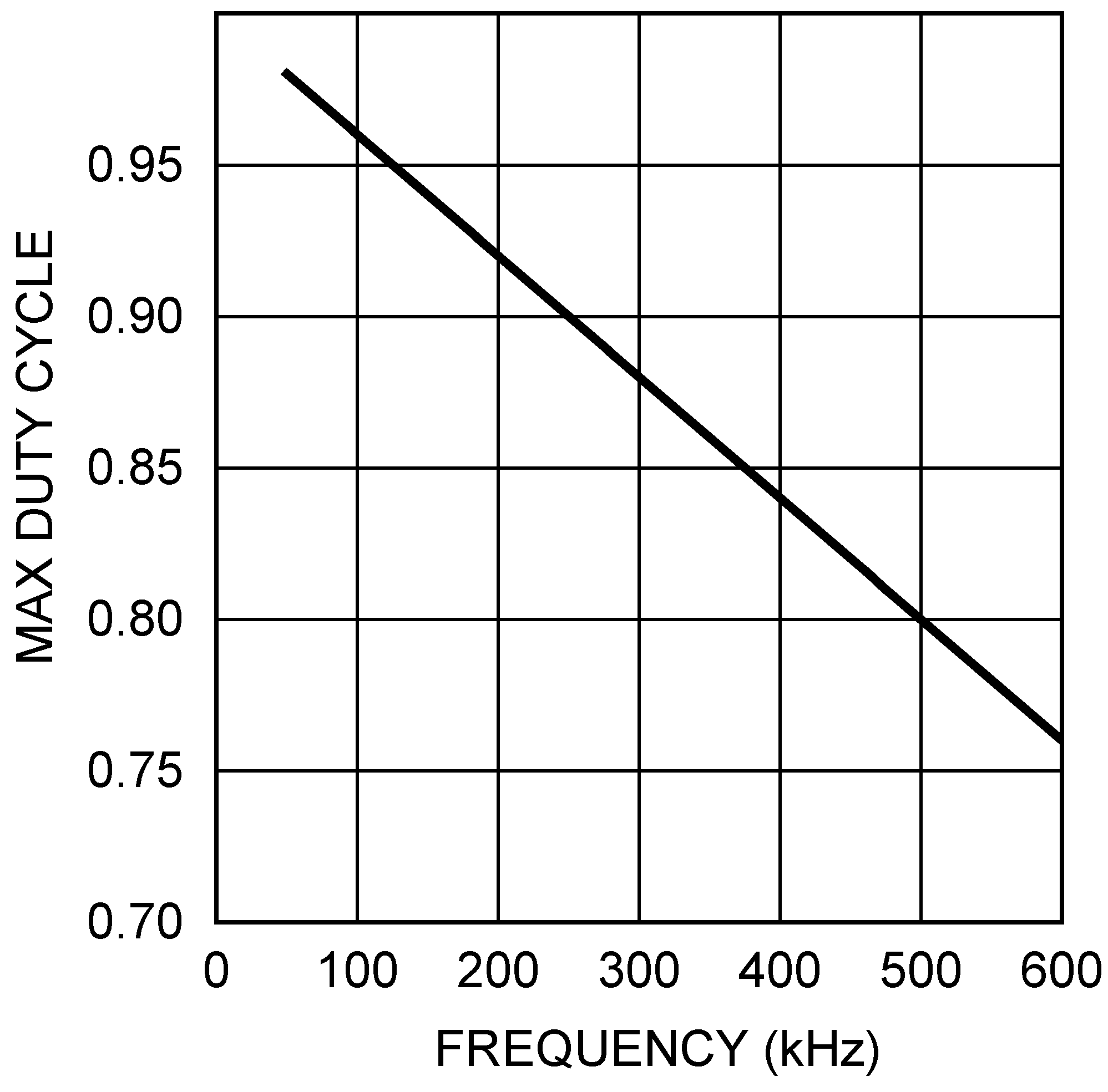 Figure 28. Maximum Duty Cycle vs Switching Frequency
7.3.12 Thermal Protection
Internal thermal shutdown circuitry is provided to protect the controller in the event the maximum junction temperature is exceeded. When activated, typically at 165°C, the controller is forced into a low power shutdown mode, disabling the output drivers and the VCC regulator. This feature is designed to prevent overheating and destroying the device.
7.4 Device Functional Modes
7.4.1 Diode Emulation
A fully synchronous buck regulator implemented with a freewheeling NMOS rather than a diode has the capability to sink current from the output in certain conditions such as light load, over-voltage or pre-bias startup. The LM5117 provides a diode emulation feature that can be enabled to prevent reverse current flow in the low-side NMOS device. When configured for diode emulation, the low-side NMOS driver is disabled when SW pin voltage is greater than -5mV during the off-time of the high-side NMOS driver, preventing reverse current flow.
A benefit of the diode emulation is lower power loss at no load or light load conditions. The negative effect of diode emulation is degraded light load transient response.
The diode emulation feature is configured with the DEMB pin. To enable diode emulation, connect the DEMB pin to GND or leave the pin floating. If continuous conduction operation is desired, the DEMB pin should be tied to a voltage greater than 3 V and may be connected to VCC. The LM5117 forces the regulator to operate in diode emulation mode when SS pin voltage is less than the internal 0.8-V reference, allowing for startup into a pre-biased load with the continuous conduction configuration.