ZHCSGG9 June 2017 LM5118-Q1
PRODUCTION DATA.
- 1 特性
- 2 应用
- 3 说明
- 4 修订历史记录
- 5 Pin Configuration and Functions
- 6 Specifications
- 7 Detailed Description
-
8 Application and Implementation
- 8.1 Application Information
- 8.2
Typical Application
- 8.2.1 Design Requirements
- 8.2.2
Detailed Design Procedure
- 8.2.2.1 Custom Design With WEBENCH® Tools
- 8.2.2.2 R7 = RT
- 8.2.2.3 Inductor Selection, L1
- 8.2.2.4 R13 = RSENSE
- 8.2.2.5 C15 = CRAMP
- 8.2.2.6 Inductor Current Limit Calculation
- 8.2.2.7 C9 - C12 = Output Capacitors
- 8.2.2.8 D1
- 8.2.2.9 D4
- 8.2.2.10 C1 - C5 = Input Capacitor
- 8.2.2.11 C20
- 8.2.2.12 C8
- 8.2.2.13 C16 = CSS
- 8.2.2.14 R8, R9
- 8.2.2.15 R1, R3, C21
- 8.2.2.16 R2
- 8.2.2.17 Snubber
- 8.2.2.18 Error Amplifier Configuration
- 8.2.3 Application Curves
- 9 Power Supply Recommendations
- 10Layout
- 11器件和文档支持
- 12机械、封装和可订购信息
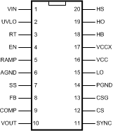
5 Pin Configuration and Functions
PWP Package
20-Pin HTSSOP
(Top View)

Pin Descriptions
| PIN | TYPE(1) | DESCRIPTION | |
|---|---|---|---|
| NO. | NAME | ||
| 1 | VIN | P/I | Input supply voltage. |
| 2 | UVLO | I | If the UVLO pin is below 1.23 V, the regulator will be in standby mode (VCC regulator running, switching regulator disabled). When the UVLO pin exceeds 1.23 V, the regulator enters the normal operating mode. An external voltage divider can be used to set an undervoltage shutdown threshold. A fixed 5-µA current is sourced out of the UVLO pin. If a current limit condition exists for 256 consecutive switching cycles, an internal switch pulls the UVLO pin to ground and then releases. |
| 3 | RT | I | The internal oscillator frequency is set with a single resistor between this pin and the AGND pin. The recommended frequency range is 50 kHz to 500 kHz. |
| 4 | EN | I | If the EN pin is below 0.5 V, the regulator will be in a low power state drawing less than 10 µA from VIN. EN must be raised above 3 V for normal operation. |
| 5 | RAMP | I | Ramp control signal. An external capacitor connected between this pin and the AGND pin sets the ramp slope used for emulated current mode control. |
| 6 | AGND | G | Analog ground. |
| 7 | SS | I | Soft Start. An external capacitor and an internal 10-µA current source set the rise time of the error amp reference. The SS pin is held low when VCC is less than the VCC undervoltage threshold (< 3.7 V), when the UVLO pin is low (< 1.23 V), when EN is low (< 0.5 V) or when thermal shutdown is active. |
| 8 | FB | I | Feedback signal from the regulated output. Connect to the inverting input of the internal error amplifier. |
| 9 | COMP | O | Output of the internal error amplifier. The loop compensation network should be connected between COMP and the FB pin. |
| 10 | VOUT | I | Output voltage monitor for emulated current mode control. Connect this pin directly to the regulated output. |
| 11 | SYNC | I | Sync input for switching regulator synchronization to an external clock. |
| 12 | CS | I | Current sense input. Connect to the diode side of the current sense resistor. |
| 13 | CSG | I | Current sense ground input. Connect to the ground side of the current sense resistor. |
| 14 | PGND | G | Power Ground. |
| 15 | LO | O | Boost MOSFET gate drive output. Connect to the gate of the external boost MOSFET. |
| 16 | VCC | P/I/O | Output of the bias regulator. Locally decouple to PGND using a low ESR/ESL capacitor located as close to the controller as possible. |
| 17 | VCCX | P/I | Optional input for an externally supplied bias supply. If the voltage at the VCCX pin is greater than 3.9 V, the internal VCC regulator is disabled and the VCC pin is internally connected to VCCX pin supply. If VCCX is not used, connect to AGND. |
| 18 | HB | I | High-side gate driver supply used in bootstrap operation. The bootstrap capacitor supplies current to charge the high-side MOSFET gate. This capacitor should be placed as close to the controller as possible and connected between HB and HS. |
| 19 | HO | O | Buck MOSFET gate drive output. Connect to the gate of the high-side buck MOSFET through a short, low inductance path. |
| 20 | HS | I | Buck MOSFET source pin. Connect to the source terminal of the high-side buck MOSFET and the bootstrap capacitor. |
| — | EP | — | Solder to the ground plane under the IC to aid in heat dissipation. |
(1) G = Ground, I = Input, O = Output, P = Power