ZHCS571I August 2010 – April 2018 LM5119
PRODUCTION DATA.
- 1 特性
- 2 应用
- 3 说明
- 4 修订历史记录
- 5 Pin Configuration and Functions
- 6 Specifications
-
7 Detailed Description
- 7.1 Overview
- 7.2 Functional Block Diagram
- 7.3
Feature Description
- 7.3.1 High Voltage Start-Up Regulator
- 7.3.2 UVLO
- 7.3.3 Enable 2
- 7.3.4 Oscillator and Sync Capability
- 7.3.5 Error Amplifiers and PWM Comparators
- 7.3.6 Ramp Generator
- 7.3.7 Current Limit
- 7.3.8 Hiccup Mode Current Limiting
- 7.3.9 Soft Start
- 7.3.10 HO and LO Output Drivers
- 7.3.11 Maximum Duty Cycle
- 7.3.12 Thermal Protection
- 7.4 Device Functional Modes
-
8 Application and Implementation
- 8.1 Application Information
- 8.2
Typical Applications
- 8.2.1
Dual-output Design Example
- 8.2.1.1 Design Requirements
- 8.2.1.2
Detailed Design Procedure
- 8.2.1.2.1 Timing Resistor
- 8.2.1.2.2 Output Inductor
- 8.2.1.2.3 Current Sense Resistor
- 8.2.1.2.4 Ramp Resistor and Ramp Capacitor
- 8.2.1.2.5 Output Capacitors
- 8.2.1.2.6 Input Capacitors
- 8.2.1.2.7 VCC Capacitor
- 8.2.1.2.8 Bootstrap Capacitor
- 8.2.1.2.9 Soft-Start Capacitor
- 8.2.1.2.10 Restart Capacitor
- 8.2.1.2.11 Output Voltage Divider
- 8.2.1.2.12 UVLO Divider
- 8.2.1.2.13 MOSFET Snubber
- 8.2.1.2.14 Error Amplifier Compensation
- 8.2.1.3 Application Curves
- 8.2.2 Two-Phase Design Example
- 8.2.1
Dual-output Design Example
- 9 Power Supply Recommendations
- 10Layout
- 11器件和文档支持
- 12机械、封装和可订购信息
7.3.7 Current Limit
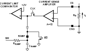
The LM5119 contains a current limit monitoring scheme to protect the regulator from possible overcurrent conditions. When set correctly, the emulated current signal is proportional to the buck switch current with a scale factor determined by the current limit sense resistor, RS, and current sense amplifier gain. The emulated signal is applied to the current limit comparator. If the emulated ramp signal exceeds 1.2 V, the present cycle is terminated (cycle-by-cycle current limiting). The current limit comparator and a simplified current measurement schematic is shown in Figure 10. In applications with small output inductance and high input voltage, the switch current may overshoot due to the propagation delay of the current limit comparator. If an overshoot must occur, the sample-and-hold circuit detects the excess recirculating current before the buck switch is turned on again. If the sample-and-hold DC level exceeds the internal current limit threshold, the buck switch is disabled and skip pulses until the current has decayed below the current limit threshold. This approach prevents current runaway conditions due to propagation delays or inductor saturation because the inductor current is forced to decay to a controlled level following any current overshoot.
 Figure 10. Current Limit and Ramp Circuit