ZHCSMW2B December 2021 – December 2022 LM5123-Q1
PRODUCTION DATA
- 1 特性
- 2 应用
- 3 说明
- 4 Revision History
- 5 说明(续)
- 6 Pin Configuration and Functions
- 7 Specifications
-
8 Detailed Description
- 8.1 Overview
- 8.2 Functional Block Diagram
- 8.3
Feature Description
- 8.3.1 Device Enable/Disable (EN, VH Pin)
- 8.3.2 High Voltage VCC Regulator (BIAS, VCC Pin)
- 8.3.3 Light Load Switching Mode Selection (MODE Pin)
- 8.3.4 VOUT Range Selection (RANGE Pin)
- 8.3.5 Line Undervoltage Lockout (UVLO Pin)
- 8.3.6 Fast Restart using VCC HOLD (VH Pin)
- 8.3.7 Adjustable Output Regulation Target (VOUT, TRK, VREF Pin)
- 8.3.8 Overvoltage Protection (VOUT Pin)
- 8.3.9 Power Good Indicator (PGOOD Pin)
- 8.3.10 Dynamically Programmable Switching Frequency (RT)
- 8.3.11 External Clock Synchronization (SYNC Pin)
- 8.3.12 Programmable Spread Spectrum (DITHER Pin)
- 8.3.13 Programmable Soft Start (SS Pin)
- 8.3.14 Wide Bandwidth Transconductance Error Amplifier and PWM (TRK, COMP Pin)
- 8.3.15 Current Sensing and Slope Compensation (CSP, CSN Pin)
- 8.3.16 Constant Peak Current Limit (CSP, CSN Pin)
- 8.3.17 Maximum Duty Cycle and Minimum Controllable On-Time Limits
- 8.3.18 Deep Sleep Mode and Bypass Operation (HO, CP Pin)
- 8.3.19 MOSFET Drivers, Integrated Boot Diode, and Hiccup Mode Fault Protection (LO, HO, HB Pin)
- 8.3.20 Thermal Shutdown Protection
- 8.4 Device Functional Modes
- 9 Application and Implementation
- 10Power Supply Recommendations
- 11Layout
- 12Device and Documentation Support
- 13Mechanical, Packaging, and Orderable Information
8.4.2.2 Diode Emulation (DE) Mode
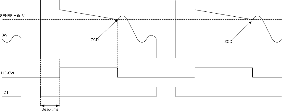
In diode emulation (DE) mode, inductor current flow is allowed only in one direction – from the input source to the output load. The device monitors the SENSE-SW voltage during the high-side switch on time and turns off the high-side switch for the remainder of the PWM cycle when the SENSE-SW voltage falls down below the 5-mV zero current detection (ZCD) threshold (VZCD). The benefit of the diode emulation is a higher efficiency than FPWM mode efficiency at light load condition.
 Figure 8-22 Zero Current Detection