ZHCSMW2B December 2021 – December 2022 LM5123-Q1
PRODUCTION DATA
- 1 特性
- 2 应用
- 3 说明
- 4 Revision History
- 5 说明(续)
- 6 Pin Configuration and Functions
- 7 Specifications
-
8 Detailed Description
- 8.1 Overview
- 8.2 Functional Block Diagram
- 8.3
Feature Description
- 8.3.1 Device Enable/Disable (EN, VH Pin)
- 8.3.2 High Voltage VCC Regulator (BIAS, VCC Pin)
- 8.3.3 Light Load Switching Mode Selection (MODE Pin)
- 8.3.4 VOUT Range Selection (RANGE Pin)
- 8.3.5 Line Undervoltage Lockout (UVLO Pin)
- 8.3.6 Fast Restart using VCC HOLD (VH Pin)
- 8.3.7 Adjustable Output Regulation Target (VOUT, TRK, VREF Pin)
- 8.3.8 Overvoltage Protection (VOUT Pin)
- 8.3.9 Power Good Indicator (PGOOD Pin)
- 8.3.10 Dynamically Programmable Switching Frequency (RT)
- 8.3.11 External Clock Synchronization (SYNC Pin)
- 8.3.12 Programmable Spread Spectrum (DITHER Pin)
- 8.3.13 Programmable Soft Start (SS Pin)
- 8.3.14 Wide Bandwidth Transconductance Error Amplifier and PWM (TRK, COMP Pin)
- 8.3.15 Current Sensing and Slope Compensation (CSP, CSN Pin)
- 8.3.16 Constant Peak Current Limit (CSP, CSN Pin)
- 8.3.17 Maximum Duty Cycle and Minimum Controllable On-Time Limits
- 8.3.18 Deep Sleep Mode and Bypass Operation (HO, CP Pin)
- 8.3.19 MOSFET Drivers, Integrated Boot Diode, and Hiccup Mode Fault Protection (LO, HO, HB Pin)
- 8.3.20 Thermal Shutdown Protection
- 8.4 Device Functional Modes
- 9 Application and Implementation
- 10Power Supply Recommendations
- 11Layout
- 12Device and Documentation Support
- 13Mechanical, Packaging, and Orderable Information
8.3.2 High Voltage VCC Regulator (BIAS, VCC Pin)
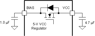
The device features a high voltage 5-V VCC regulator, which is sourced from the BIAS pin. The internal VCC regulator turns on 50 μs after the device is enabled, and 120-μs device configuration starts when VCC is above VCC UVLO threshold (VVCC-UVLO). The device configuration is reset when the device shuts down or VCC falls down below 2.2 V. The preferred way to reconfigure the device is to shut down the device. During configuration time, the light load switching mode and VOUT range are selected.
The high voltage VCC regulator allows the connection of the BIAS pin directly to supply voltages from 3.8 V to 42 V. When BIAS is less than the 5-V VCC regulation target (VVCC-REG), the VCC output tracks the BIAS pin voltage with a small dropout voltage which is caused by 1.7-Ω resistance of the VCC regulator.
The recommended VCC capacitor value is 4.7 μF. The VCC capacitor should be populated between VCC and PGND as close to the device. The recommended BIAS capacitor value is 1.0 μF. The BIAS capacitor must be populated between BIAS and PGND close to the device.
 Figure 8-2 High Voltage VCC
Regulator
Figure 8-2 High Voltage VCC
RegulatorThe VCC regulator features a VCC current limit function that prevents device damage when the VCC pin is shorted to ground accidentally. The minimum sourcing capability of the VCC regulator is 100 mA (IVCC-CL) during either the device configuration time or active mode operation. The minimum sourcing capability of the VCC regulator is reduced to 1 mA during sleep mode or deep sleep mode, or when EN is less than VEN and VH is greater than VSYNC. The VCC regulator supplies the internal drivers and other internal circuits. The external MOSFETs must be carefully selected to make the driver current consumption less than IVCC-CL. The driver current consumption can be calculated in Equation 1.
where
- QG@5V is the N-channel MOSFET gate charge at 5 V gate-source voltage.
If VIN operation below 3.8 V is required, the BIAS pin must be connected to the output of the boost converter (VLOAD). By connecting the BIAS pin to VLOAD, the boost converter input voltage (VSUPPLY) can drop down to 0.8 V if BIAS is greater than 3.8 V. See Section 8.3.17 for more detailed information about the minimum VSUPPLY.