ZHCSEL1C May 2012 – Februrary 2016 LM5134
PRODUCTION DATA.
- 1 特性
- 2 应用
- 3 说明
- 4 修订历史记录
- 5 Pin Configuration and Functions
- 6 Specifications
- 7 Detailed Description
- 8 Application and Implementation
- 9 Power Supply Recommendations
- 10Layout
- 11器件和文档支持
- 12机械、封装和可订购信息
5 Pin Configuration and Functions
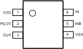
DBV Package, NGG Package
6-Pin SOT-23, 6-Pin WSON
Top View

Pin Functions
| PIN | I/O | DESCRIPTION | APPLICATION INFORMATION | |
|---|---|---|---|---|
| NAME | NO. | |||
| VDD | 1 | — | Gate drive supply | Locally decouple to VSS using low ESR/ESL capacitor located as close as possible to the IC. |
| PILOT | 2 | O | Gate drive output for an external turnoff FET | Connect to the gate of a small turnoff MOSFET with a short, low inductance path. The turnoff FET provides a local turnoff path. |
| OUT | 3 | O | Gate drive output for the power FET | Connect to the gate of the power FET with a short, low inductance path. A gate resistor can be used to eliminate potential gate oscillations. |
| VSS | 4 | — | Ground | All signals are referenced to this ground. |
| INB | 5 | I | Inverting logic input | Connect to VSS when not used. |
| IN | 6 | I | Non-inverting logic input | Connect to VDD when not used. |
| EP | EP | — | Exposed Pad | It is recommended that the exposed pad on the bottom of the package be soldered to ground plane on the PC board, and that ground plane extend out from beneath the IC to help dissipate heat. |