ZHCSFB5D July 2016 – December 2017 LM5141-Q1
PRODUCTION DATA.
- 1 特性
- 2 应用
- 3 说明
- 4 修订历史记录
- 5 Pin Configuration and Functions
- 6 Specifications
-
7 Detailed Description
- 7.1 Overview
- 7.2 Functional Block Diagram
- 7.3
Feature Description
- 7.3.1 High Voltage Start-up Regulator
- 7.3.2 VCC Regulator
- 7.3.3 Oscillator
- 7.3.4 Synchronization
- 7.3.5 Frequency Dithering (Spread Spectrum)
- 7.3.6 Enable
- 7.3.7 Power Good
- 7.3.8 Output Voltage
- 7.3.9 Current Sense
- 7.3.10 DCR Current Sensing
- 7.3.11 Error Amplifier and PWM Comparator
- 7.3.12 Slope Compensation
- 7.3.13 Hiccup Mode Current Limiting
- 7.3.14 Standby Mode
- 7.3.15 Soft Start
- 7.3.16 Diode Emulation
- 7.3.17 High- and Low-Side Drivers
-
8 Application and Implementation
- 8.1 Application Information
- 8.2 Typical Application
- 9 Power Supply Recommendations
- 10Layout
- 11器件和文档支持
- 12机械、封装和可订购信息
7.3.13 Hiccup Mode Current Limiting
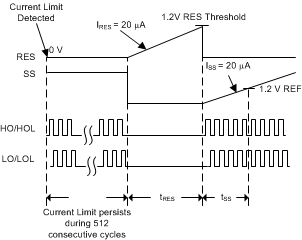
The LM5141-Q1 includes an optional hiccup mode protection function that is enabled when a capacitor is connected to the RES pin. In normal operation the RES capacitor is discharged to ground. If 512 consecutive cycles of cycle-by-cycle current limiting occur, the SS pin capacitor is pulled low and the HO and LO outputs are disabled (refer to Figure 26). A 20-μA current source begins to charge the RES capacitor.
When the RES pin charges to 1.2 V, the RES pin is pulled low, and the SS capacitor begins to charge. The 512 cycle hiccup counter is reset if 4 consecutive switching cycles occur without exceeding the current limit threshold. The controller is in forced PWM (FPWM) continuous conduction mode when the DEMB pin is connected to VDDA. In this mode the SS pin is clamped to a level 200 mV above the feedback voltage to the internal error amplifier. This ensures that SS can be pulled low quickly during a brief overcurrent event and prevent overshoot of VOUT when the overcurrent condition is removed.
If DEMB = 0 V, the controller operates in diode emulation with light loads (discontinuous conduction mode) and the SS pin is allowed to charge to VDDA. This reduces the quiescent current of the LM5141-Q1. If 32 or more cycle-by-cycle current limit events occur, the SS pin is clamped to 200 mV above the feedback voltage to the internal error amplifier until the hiccup counter is reset. Thus, if a momentary overload occurs that causes at least 32 cycles of current limiting, the SS capacitor voltage will be slightly higher than the FB voltage and will control VOUT during overload recovery.
 Figure 26. Hiccup Mode