ZHCSFB5D July 2016 – December 2017 LM5141-Q1
PRODUCTION DATA.
- 1 特性
- 2 应用
- 3 说明
- 4 修订历史记录
- 5 Pin Configuration and Functions
- 6 Specifications
-
7 Detailed Description
- 7.1 Overview
- 7.2 Functional Block Diagram
- 7.3
Feature Description
- 7.3.1 High Voltage Start-up Regulator
- 7.3.2 VCC Regulator
- 7.3.3 Oscillator
- 7.3.4 Synchronization
- 7.3.5 Frequency Dithering (Spread Spectrum)
- 7.3.6 Enable
- 7.3.7 Power Good
- 7.3.8 Output Voltage
- 7.3.9 Current Sense
- 7.3.10 DCR Current Sensing
- 7.3.11 Error Amplifier and PWM Comparator
- 7.3.12 Slope Compensation
- 7.3.13 Hiccup Mode Current Limiting
- 7.3.14 Standby Mode
- 7.3.15 Soft Start
- 7.3.16 Diode Emulation
- 7.3.17 High- and Low-Side Drivers
-
8 Application and Implementation
- 8.1 Application Information
- 8.2 Typical Application
- 9 Power Supply Recommendations
- 10Layout
- 11器件和文档支持
- 12机械、封装和可订购信息
8.2.2.5.3 Driver Slew-Rate Control
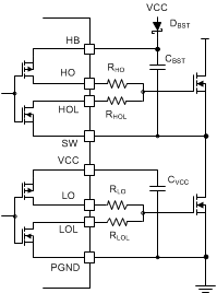
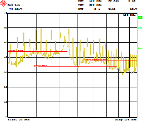
Figure 30 shows the high current driver outputs with independent source and current sink pins for slew-rate control. Slew-rate control enables the user to adjust the switch node rise and fall times which can reduce the conducted EMI in the FM radio band (30 MHz to 108 MHz). Using the LM5141-Q1 EVM, conducted emissions were measured in accordance with CISPR 25 Class 5. Figure 31 shows the measured results without slew-rate control.
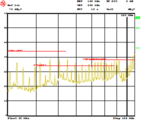
The conducted EMI results with slew-rate control are shown in Figure 32, a 10-dB reduction in conduction emissions in the FM band is attained by using slew-rate control. This can help reduce the size and cost of the EMI filters.
 Figure 30. Drivers With Slew-Rate Control
 Figure 31. EMI Measurements CISPR 25 Class 5, Without Slew-Rate Control
 Figure 32. EMI Measurements CISPR 25 With Slew-Rate Control