ZHCSG18 March 2017 LM5141
PRODUCTION DATA.
- 1 特性
- 2 应用
- 3 说明
- 4 修订历史记录
- 5 Pin Configuration and Functions
- 6 Specifications
-
7 Detailed Description
- 7.1 Overview
- 7.2 Functional Block Diagram
- 7.3
Feature Description
- 7.3.1 High Voltage Start-up Regulator
- 7.3.2 VCC Regulator
- 7.3.3 Oscillator
- 7.3.4 Synchronization
- 7.3.5 Frequency Dithering (Spread Spectrum)
- 7.3.6 Enable
- 7.3.7 Power Good
- 7.3.8 Output Voltage
- 7.3.9 Current Sense
- 7.3.10 DCR Current Sensing
- 7.3.11 Error Amplifier and PWM Comparator
- 7.3.12 Slope Compensation
- 7.3.13 Hiccup Mode Current Limiting
- 7.3.14 Standby Mode
- 7.3.15 Soft-Start
- 7.3.16 Diode Emulation
- 7.3.17 High and Low Side Drivers
- 8 Application and Implementation
- 9 Power Supply Recommendations
- 10Layout
- 11器件和文档支持
- 12机械、封装和可订购信息
6 Specifications
6.1 Absolute Maximum Ratings
over operating free-air temperature range (unless otherwise noted)(1)| MIN | MAX | UNIT | ||
|---|---|---|---|---|
| Input voltage | VIN | –0.3 | 70 | V |
| SW to PGND | –0.3 | 70 | V | |
| SW to PGND (20 ns transient) | –5 | V | ||
| HB to SW | –0.3 | 6.5 | V | |
| HB to SW (20 ns transient) | –5 | V | ||
| HO, HOL to SW | –0.3 | HB + 0.3 | V | |
| HO, HOL to SW (20 ns transient) | –5 | V | ||
| LO, LOL to PGND | –0.3 | VCC + 0.3 | V | |
| LO, LOL to PGND (20 ns transient) | –1.5 | V | ||
| OSC, SS, COMP, RES, DEMB, RT, DITH | –0.3 | VDD + 0.3 | V | |
| EN to PGND | –0.3 | 70 | V | |
| VCC, VCCX, VDD, PG, FB | –0.3 | 6.5 | V | |
| VOUT, CS | –0.3 | 15.5 | V | |
| PGND to AGND | –0.3 | 0.3 | V | |
| Operating junction temperature(2) | –40 | 150 | °C | |
| Storage temperature, Tstg | –65 | 150 | °C | |
(1) Stresses beyond those listed under Absolute Maximum Ratings may cause permanent damage to the device. These are stress ratings only, which do not imply functional operation of the device at these or any other conditions beyond those indicated under Recommended Operating Conditions. Exposure to absolute-maximum-rated conditions for extended periods may affect device reliability.
(2) High junction temperatures degrade operating lifetimes. Operating lifetime is de-rated for junction temperatures greater than 125°C.
6.2 ESD Ratings
| VALUE | UNIT | |||
|---|---|---|---|---|
| V(ESD) | Electrostatic discharge | Human-body model (HBM), per ANSI/ESDA/JEDEC JS-001(1) | ±2000 | V |
| Charged-device model (CDM), per JEDEC specification JESD22-C101(2) | ±500 | |||
(1) JEDEC document JEP155 states that 500-V HBM allows safe manufacturing with a standard ESD control process.
(2) JEDEC document JEP157 states that 250-V CDM allows safe manufacturing with a standard ESD control process.
6.3 Recommended Operating Conditions
over operating free-air temperature range (unless otherwise noted)(1)| MIN | NOM | MAX | UNIT | |||
|---|---|---|---|---|---|---|
| VIN | Input voltage | VIN | 3.8 | 65 | V | |
| SW to PGND | –0.3 | 65 | V | |||
| HB to SW | –0.3 | 5 | 5.25 | V | ||
| HO, HOL to SW | –0.3 | HB + 0.3 | V | |||
| LO, LOL to PGND | –0.3 | 5 | 5.25 | V | ||
| FB, PG, OSC, SS, RES, DEMB, VCCX | –0.3 | 5 | V | |||
| EN to PGND | –0.3 | 65 | V | |||
| VCC, VDD | –0.3 | 5 | 5.25 | V | ||
| VOUT, CS | 1.5 | 5 | 15 | V | ||
| PGND to AGND | –0.3 | 0.3 | V | |||
| Operating junction temperature(2) | –40 | 125 | °C | |||
(1) Recommended Operating Conditions are conditions under which the device is intended to be functional. For specifications and test conditions, see Electrical Characteristics.
(2) High junction temperatures degrade operating lifetimes. Operating lifetime is de-rated for junction temperatures greater than 125°C.
6.4 Thermal Information
| THERMAL METRIC(1) | LM5141 | UNIT | |
|---|---|---|---|
| RGE (QFN) | |||
| 24 PINS | |||
| RθJA | Junction-to-ambient thermal resistance | 34.1 | °C/W |
| RθJC(top) | Junction-to-case (top) thermal resistance | 36.8 | °C/W |
| RθJB | Junction-to-board thermal resistance | 12.1 | °C/W |
| ψJT | Junction-to-top characterization parameter | 0.5 | °C/W |
| ψJB | Junction-to-board characterization parameter | 12.2 | °C/W |
| RθJC(bot) | Junction-to-case (bottom) thermal resistance | 2.9 | °C/W |
(1) For more information about traditional and new thermal metrics, see the Semiconductor and IC Package Thermal Metrics application report.
6.5 Electrical Characteristics
TJ = –40°C to +125°C, Typical values TJ = 25°C, VIN = 12 V, VCCX = 5 V, VOUT = 5 V, EN = 5 V, OSC = VDD, FSW = 2.2 MHz, no-load on the Drive Outputs (HO, HOL, LO, and LOL outputs), over operating free-air temperature range (unless otherwise noted)(1)(2)| PARAMETER | TEST CONDITIONS | MIN | TYP | MAX | UNIT | |
|---|---|---|---|---|---|---|
| VIN SUPPLY VOLTAGE | ||||||
| ISHUTDOWN | Shutdown mode current | VIN = 8–18 V, EN = 0 V, VCCX = 0 V | 10 | 12.5 | µA | |
| ISTANDBY | Standby current | EN = 5 V, FB = VDD, VOUT in regulation, no-load, not switching, DEMB = GND. | 35 | 45 | µA | |
| EN = 5 V, FB = 0 V, VOUT in regulation, no-load, not switching, VCCX = 5 V, DEMB = GND. | 42 | 55 | ||||
| VCC REGULATOR | ||||||
| VCC(REG) | VCC regulation voltage | VIN = 6–18 V, 0–75 mA, VCCX = 0 V | 4.75 | 5 | 5.25 | V |
| VCC(UVLO) | VCC under voltage threshold | VCC rising, VCCX = 0 V | 3.25 | 3.4 | 3.55 | V |
| VCC(HYST) | VCC hysteresis voltage | VCCX = 0 V | 175 | mV | ||
| ICC(LIM) | VCC sourcing current limit | VCCX = 0 V | 85 | 125 | mA | |
| VDDA | ||||||
| VDDA(REG) | Internal bias supply power | VCCX = 0 V | 4.75 | 5 | 5.25 | V |
| VDDA(UVLO) | VCC rising, VCCX = 0 V | 3.1 | 3.2 | 3.3 | V | |
| VDDA(HYST) | VCCX = 0 V | 125 | mV | |||
| RVDDA | VCCX = 0 V | 55 | Ω | |||
| VCCX | ||||||
| VCCX(ON) | VCC rising | 4.1 | 4.3 | 4.4 | V | |
| VCCX(HYST) | 80 | mV | ||||
| R(VCCX) | VCCX = 5 V | 2 | Ω | |||
| OSCILLATOR SELECT THRESHOLDS | ||||||
| Oscillator select threshold 2.2 MHz | (OSC pin) | 2.0 | V | |||
| Oscillator select threshold 440 kHz | (OSC pin) | 0.8 | V | |||
| CURENT LIMIT | ||||||
| V(CS) | Current limit threshold | ILSET = VDDA, measure from CS to VOUT | 68 | 75 | 82 | mV |
| tdly | Current sense delay to output | 40 | ns | |||
| Current sense amplifier gain | 11.4 | 12 | 12.6 | V/V | ||
| ICS(BIAS) | Amplifier input bias | 10 | nA | |||
| RES | ||||||
| I(RES) | RES current source | 20 | µA | |||
| V(RES) | RES threshold | 1.2 | V | |||
| Timer | Timer hiccup mode fault | 512 | cycles | |||
| RDS(ON) | RES pull-down | 4 | Ω | |||
| OUTPUT VOLTAGE REGULATION | ||||||
| 3.3 V | VIN = 3.8–42 V | 3.273 | 3.3 | 3.327 | V | |
| 5 V | VIN = 5.5–42 V | 4.96 | 5.0 | 5.04 | V | |
| FEEDBACK | ||||||
| VOUT select threshold 3.3 V | VDD - 0.3 | V | ||||
| Regulated feedback voltage | 1.193 | 1.2 | 1.207 | V | ||
| FB(LOWRES) | Resistance to ground on FB for FB = 0 detection | 500 | Ω | |||
| FB(EXTRES) | Thevenin equivalent resistance at FB for external regulation detection | FB < 2 V | 5 | kΩ | ||
| TRANSCONDUCTANCE AMPLIFIER | ||||||
| Gm | Gain | Feedback to COMP | 1010 | 1200 | µS | |
| Input bias current | 15 | nA | ||||
| Transconductance Amplifier source current | COMP = 1 V, FB = 1 V | 100 | µA | |||
| Transconductance Amplifier sink current | COMP = 1 V, FB = 1.4 V | 100 | µA | |||
| POWER GOOD | ||||||
| PG(UV) | PG under voltage trip levels | Falling with respect to the regulation voltage | 90% | 92% | 94% | |
| PG(OVP) | PG over voltage trip levels | Rising with respect to the regulation voltage | 108% | 110% | 112% | |
| PG(HYST) | 3.4% | |||||
| PG(VOL) | PG | Open collector, Isink = 2 mA | 0.4 | V | ||
| PG(rdly) | OV filter time | VOUT rising | 25 | µs | ||
| PG(fdly) | UV filter time | VOUT falling | 30 | µs | ||
| HO GATE DRIVER | ||||||
| VOLH | HO Low-state output voltage | IHO = 100 mA | 0.05 | V | ||
| VOHH | HO High-state output voltage | IHO = –100 mA, VOHH = VHB - VHO | 0.07 | V | ||
| trHO | HO rise time (10% to 90%) | CLOAD = 2700 pf | 4 | ns | ||
| tfHO | HO fall time (90% to 10%) | CLOAD = 2700 pf | 3 | ns | ||
| IOHH | HO peak source current | VHO = 0 V, SW = 0 V, HB = 5 V, VCCX = 5 V | 3.25 | Apk | ||
| IOLH | HO peak sink current | VCCX = 5 V | 4.25 | Apk | ||
| V(BOOT) | UVLO | HO falling | 2.5 | V | ||
| Hysteresis | 110 | mV | ||||
| I(BOOT) | Quiescent current | 3 | µA | |||
| LO GATE DRIVER | ||||||
| VOLL | LO Low-state output voltage | ILO = 100 mA | 0.05 | V | ||
| VOHL | LO High-state output voltage | ILO = –100 mA, VOHL = VCC - VLO | 0.07 | V | ||
| trLO | LO rise time (10% to 90%) | CLOAD = 2700 pf | 4 | ns | ||
| tfLO | LO fall time (90% to 10%) | CLOAD = 2700 pf | 3 | ns | ||
| IOHL | LO peak source current | VCCX = 5 V | 3.25 | Apk | ||
| IOLL | LO peak sink current | VCCX = 5 V | 4.25 | Apk | ||
| ADAPTIVE DEAD TIME CONTROL | ||||||
| V(GS-DET) | VGS detection threshold | VGS falling, no-load | 2.5 | V | ||
| tdly1 | HO off to LO on dead time | 20 | 40 | ns | ||
| tdly2 | LO off to HO on dead time | 20 | 38 | ns | ||
| DIODE EMULATION | ||||||
| VIL | DEMB input low threshold | 0.8 | V | |||
| VIH | FPWM input high threshold | 2.0 | V | |||
| SW | Zero cross threshold | –5 | mV | |||
| ENABLE INPUT | ||||||
| VIL | Enable input low threshold | VCCX = 0 V | 0.8 | V | ||
| VIH | Enable input high threshold | VCCX = 0 V | 2.0 | V | ||
| IIkg | Leakage | EN logic input only | 1 | µA | ||
| SYN INPUT (DEMB pin) | ||||||
| VIL | DEMB input low threshold | 0.8 | V | |||
| VIH | DEMB input high threshold | 2.0 | V | |||
| DEMB input low frequency range 440 kHz | 350 | 550 | kHz | |||
| DEMB input high frequency range 2.2 MHz | 1800 | 2600 | kHz | |||
| DITHER | ||||||
| IDITHER | Dither source/sink current | 20 | µA | |||
| VDITHER | Dither high threshold | 1.26 | V | |||
| Dither low threshold | 1.14 | V | ||||
| SOFT-START | ||||||
| ISS | Soft-Start current | 16 | 22 | 28 | µA | |
| RDS(ON) | Soft-Start pull-down resistance | 3 | Ω | |||
| THERMAL | ||||||
| TSD Thermal Shutdown | 175 | ºC | ||||
| Thermal shutdown hysteresis | 15 | ºC | ||||
(1) All minimum and maximum limits are specified by correlating the electrical characteristics to process and temperature variations and applying statistical process control.
(2) The junction temperature (TJ in ºC) is calculated from the ambient temperature (TA in ºC) and power dissipation (PD in Watts) as follows: TJ = TA + (PD × RθJA) where RθJA (in °C/W) is the package thermal impedance provided in the Thermal Information section.
6.6 Switching Characteristics
over operating free-air temperature range (unless otherwise noted)| PARAMETER | TEST CONDITIONS | MIN | TYP | MAX | UNIT | ||
|---|---|---|---|---|---|---|---|
| Oscillator Frequency 2.2 MHz | OSC = VDDA, VIN = 8–18 V | 2100 | 2200 | 2300 | kHz | ||
| Oscillator Frequency 440 kHz | OSC = GND, VIN = 8–18 V | 420 | 440 | 460 | kHz | ||
| RT | Adjustment Range | Minimum | OSC = VDD, RTMIN = 61.9 kΩ | 1710 | 1800 | 1890 | kHz |
| Typical | OSC = VDD, RTTYP = 49.9 kΩ | 2100 | 2200 | 2300 | kHz | ||
| 2.2 MHz | Maximum | OSC = VDD, RTMAX = 43.2 kΩ | 2405 | 2530 | 2655 | kHz | |
| RT | Adjustment Range | Minimum | OSC = GND, RTMIN = 73.2 k | 285 | 300 | 315 | kHz |
| Typical | OSC = GND, RTTYP = 49.9 kΩ | 420 | 440 | 460 | kHz | ||
| 440 kHz | Maximum | OSC = GND, RTMAX = 44.2 kΩ | 475 | 500 | 525 | kHz | |
| RT | Response time | RT= 61.9–43.2 kΩ | 2 | µs | |||
| RT | Response time | RT = 43.2–61.9 kΩ | 3.5 | µs | |||
| RT | Response time | 16 | µs | ||||
| ton | Minimum on-time | 45 | 66 | ns | |||
| toff | Minimum off-time | 100 | ns | ||||
6.7 Typical Characteristics
At TA = 25ºC, unless otherwise noted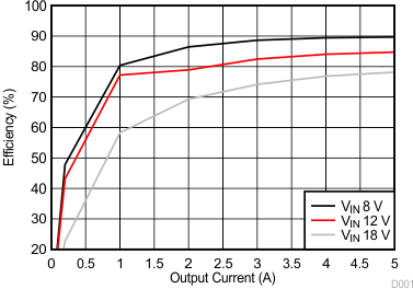
| VIN 8–18 V | EN = 12 V | 2.2 MHz |
| VOUT 5 V | FPWM |
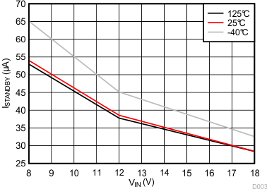
| EN = 12 V |
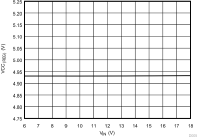
| VIN 6-18 V | EN = GND |
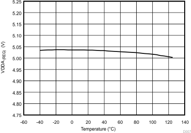
| VCC Rising | EN = 12 V |
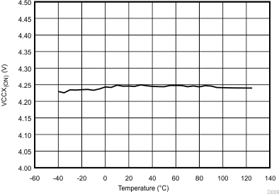
| VCC Rising | EN = 12 V |
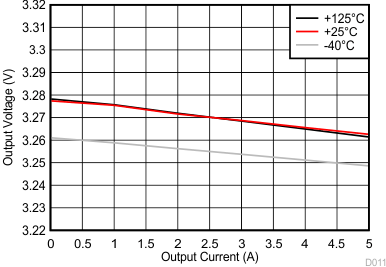
| VIN 12 V | FB = VDDA | EN = 12 V |
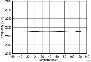
| VIN 12 V | EN = 12 V | OSC = VDDA |
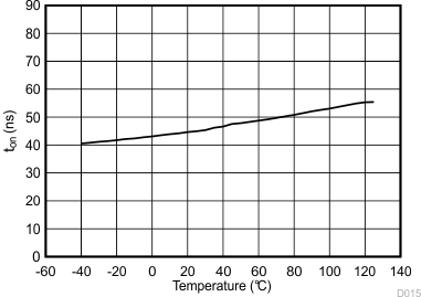
| VIN 18 V |
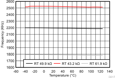
| VIN 12 V |
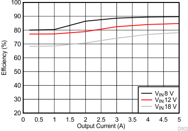
| VIN 8–18 V | EN = 12 V | 2.2 MHz |
| VOUT 5 V | DEMB |
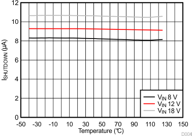
| VIN 8–18 V | EN = 0 V |
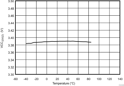
| VIN 8–18 V | EN = 12 V |
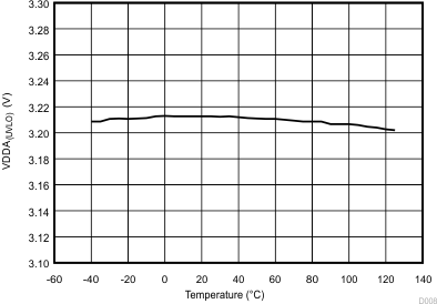
| VCC Rising | EN = 12 V |
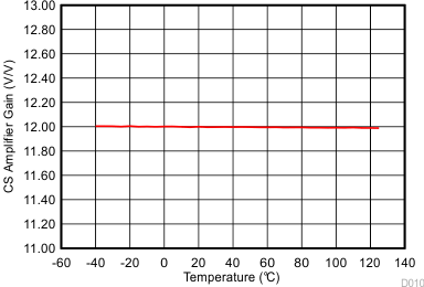
| VIN 12 V | EN = 12 V |
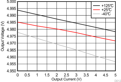
| VIN 12 V | EN = 12 V | FB = GND |
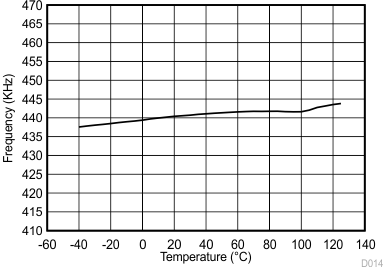
| VIN 12 V | EN = 12 V | OSC = AGND |
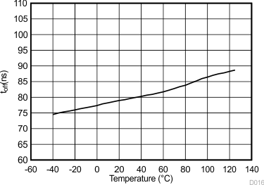
| VIN 3.8 V | VOUT 3.3 V |
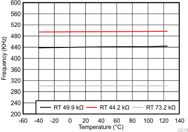
| VIN 12 V |