ZHCSG18 March 2017 LM5141
PRODUCTION DATA.
- 1 特性
- 2 应用
- 3 说明
- 4 修订历史记录
- 5 Pin Configuration and Functions
- 6 Specifications
-
7 Detailed Description
- 7.1 Overview
- 7.2 Functional Block Diagram
- 7.3
Feature Description
- 7.3.1 High Voltage Start-up Regulator
- 7.3.2 VCC Regulator
- 7.3.3 Oscillator
- 7.3.4 Synchronization
- 7.3.5 Frequency Dithering (Spread Spectrum)
- 7.3.6 Enable
- 7.3.7 Power Good
- 7.3.8 Output Voltage
- 7.3.9 Current Sense
- 7.3.10 DCR Current Sensing
- 7.3.11 Error Amplifier and PWM Comparator
- 7.3.12 Slope Compensation
- 7.3.13 Hiccup Mode Current Limiting
- 7.3.14 Standby Mode
- 7.3.15 Soft-Start
- 7.3.16 Diode Emulation
- 7.3.17 High and Low Side Drivers
- 8 Application and Implementation
- 9 Power Supply Recommendations
- 10Layout
- 11器件和文档支持
- 12机械、封装和可订购信息
8 Application and Implementation
NOTE
Information in the following applications sections is not part of the TI component specification, and TI does not warrant its accuracy or completeness. TI’s customers are responsible for determining suitability of components for their purposes. Customers should validate and test their design implementation to confirm system functionality.
8.1 Application Information
The LM5141 is a synchronous buck controller used to convert a higher input voltage to a lower output voltage. The following design procedure can be used to select external component values. Alternately, the WEBENCH® software may be used to generate a complete design. The WEBENCH software uses an iterative design procedure and accesses a comprehensive database of components when generating a design. This section presents a simplified design process. In addition to the WEBENCH software the LM5141ADESIGN-CALC.xls quick start Excel calculator is available at www.ti.com.
8.2 Typical Application
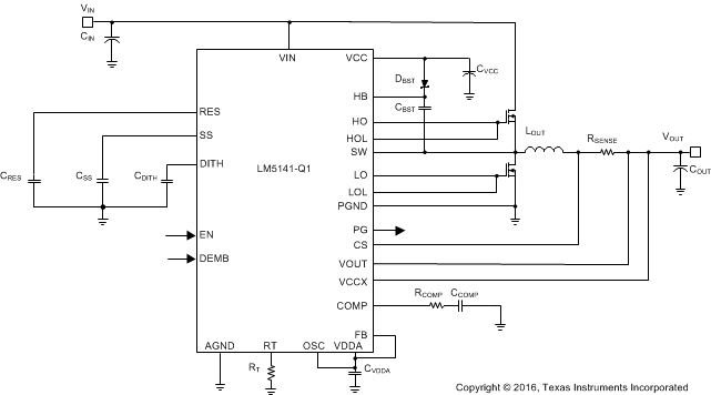 Figure 28. Typical Application Schematic
8.2.1 Design Requirements
For this design example, the intended input, output, and performance parameters are shown in Table 2.
Table 3. Design Requirements
| DESIGN PARAMETER | EXAMPLE VALUE |
|---|---|
| Input voltage range (Steady State) | 8 V to 18 V |
| VIN maximum (Transient) | 42 V |
| VIN minimum (Cold Crank) | 3.8 V |
| Output voltage | 3.3 V |
| Output current | 6 A |
| Operating frequency | 2.2 MHz |
| Output voltage regulation | ±1% |
| Standby current, one output enabled, no-load | < 35 µA |
| Shutdown Current | 10 µA |
8.2.2 Detailed Design Procedure
8.2.2.1 Custom Design With WEBENCH® Tools
Click here to create a custom design using the LM5141 device with the WEBENCH® Power Designer.
- Start by entering the input voltage (VIN), output voltage (VOUT), and output current (IOUT) requirements.
- Optimize the design for key parameters such as efficiency, footprint, and cost using the optimizer dial.
- Compare the generated design with other possible solutions from Texas Instruments.
The WEBENCH Power Designer provides a customized schematic along with a list of materials with real-time pricing and component availability.
In most cases, these actions are available:
- Run electrical simulations to see important waveforms and circuit performance
- Run thermal simulations to understand board thermal performance
- Export customized schematic and layout into popular CAD formats
- Print PDF reports for the design, and share the design with colleagues
Get more information about WEBENCH tools at www.ti.com/WEBENCH.
- Buck Inductor value
- Calculate the peak inductor current
- Current Sense resistor value
- Output capacitor value
- Input filter
- MOSFET selection
- Control Loop design
8.2.3 Inductor Calculation
For peak current mode control, sub-harmonic oscillation occurs with a duty cycle greater than 50% and is characterized by alternating wide and narrow pulses at the SW pin. By adding a slope compensating ramp equal to at least one-half the inductor current down-slope, any tendency toward sub-harmonic oscillation is damped within one switching cycle. For design simplification, the LM5141 has an internal slope compensation ramp added to the current sense signal.
For the slope compensation ramp to dampen sub-harmonic oscillation, the inductor value should be calculated based on the following guidelines (equation 15 assumes an inductor ripple current 30%):

- Lower inductor values increase the peak-to-peak inductor current, which minimizes size and cost and improves transient response at the expense of reduced efficiency due to higher peak currents.
- Higher inductance values decrease the peak-to-peak inductor current, which typically increases efficiency by reducing the RMS current but requires larger output capacitors to meet load-transient specifications.


A standard inductor value of 1.5 µH was selected


The peak-to-peak inductor current is:


8.2.4 Current Sense Resistor
When calculating the current sense resistor, the maximum output current capability (IOUT(MAX)) should be at least 20% higher than the required full load current to account for tolerances, ripple current, and load transients. For this example, 120% of the 6.41 A peak inductor current calculated in the previous section (Ipk) is 7.69 A. The current sense resistor value can be calculated using:


where
- V(CS) is the 75 mV current limit threshold
The RSENSE value selected is 9 mΩ
Carefully observe the PCB layout guidelines to ensure that noise and DC errors do not corrupt the differential current sense signals between the CS and VOUT pins. Place the sense resistor close to the devices with short, direct traces, creating Kelvin-sense connections between the current-sense resistor and the LM5141.
The propagation delays through the current limit comparator, logic, and external MOSFET gate drivers allow the peak current to increase above the calculated current limit threshold. For a propagation delay of tdly, the worst case peak current through the inductor with the output shorted can be calculated from:

From the Electrical Characterization Table, tdly is typically 40 ns.
Once the peak current and the inductance parameters are known, the inductor can be chosen. An inductor with a saturation current greater than IpkSCKT (8.81 Apk) should be selected.
8.2.5 Output Capacitor
In a switch mode power supply, the minimum output capacitance is typically selected based on the capacitor ripple current rating and the load transient requirements. The output capacitor must be large enough to absorb the inductor energy and limit over voltage when transitioning from full-load to no-load, and to limit the output voltage undershoot during no-load to full load transients. The worst-case load transient from zero to full load occurs when the input voltage is at the maximum value and a current switching cycle has just finished. The total output voltage drop ΔVOUT is the sum of the voltage drop while the inductor is ramping up to support the full load and the voltage drop before the next pulse can occur.
The output capacitance required to maintain the minimum output voltage drop (ΔVOUT) can be calculated as follows:


where
- ISTEP = 4 A
- ΔVOUT = 1% of 3.3 V, or 33 mV
For this example a total of 211 μF of capacitance is used, two 82-μF aluminum capacitors for energy storage and one 47 μF low ESR ceramic capacitor to reduce high frequency noise.
Generally, when sufficient capacitance is used to satisfy the undershoot requirement, the overshoot during a full-load to no-load transient will also be satisfactory. After the output capacitance has been selected, calculate the output ripple current and verify that the ripple current is within the capacitor ripple current ratings.

8.2.6 Input Filter
A power supply input typically has a relatively high source impedance at the switching frequency. Good quality input capacitors are necessary to limit the ripple voltage at the VIN pin while supplying most of the switch current during the buck switch on-time. When the buck switch turns on, the current drawn from the input capacitor steps from zero to the valley of the inductor current waveform, then ramps up to the peak value, and then drops to the zero at turn-off.
Average input current can be calculated from the total input power required to support the load at VOUT:

The efficiency (η) is assumed to be 83% for this design example, yielding a total input power:


The input capacitors should be selected with sufficient RMS current rating and the maximum voltage rating.


8.2.6.1 EMI Filter Design
EMI Filter Design Steps:
- Calculate the required attenuation
- Capacitor CIN represents the existing capacitor at the input of the switching converter (10 µF was used for this application)
- Inductor LF is usually selected between 1 μH and 10 μH (1.8 µH was used for this application), but can be smaller to reduce losses in a high current design
- Calculate capacitor CF
 Figure 29. Input EMI Filter
By calculating the first harmonic current from the Fourier series of the input current waveform and multiplying it by the input impedance (the impedance is defined by the existing input capacitor CIN), a formula can be derived to obtain the required attenuation:


VMAX is the allowed dBμV noise level for the particular EMI standard. CIN is the existing input capacitors of the Buck converter, for this application 10 µF was selected. DMAX is the maximum duty cycle, Ipk is the inductor current, the current at the input can be modeled as a square wave, FSW is the switching frequency.


For this application, CF was chosen to be 1 μF. Adding an input filter to a switching regulator modifies the control-to output transfer function. The output impedance of the filter must be sufficiently small such that the input filter does not significantly affect the loop gain of the buck converter. The impedance of the filter peaks at the filter resonant frequency.


Referring to Figure 29, the purpose of RD is to reduce the peak output impedance of the filter at the cutoff frequency. The capacitor CD blocks the dc component of the input voltage, and avoids excessive power dissipation on RD. The capacitor CD should have lower impedance than RD at the resonant frequency, with a capacitance value greater than 5 times the filter capacitor CIN. This will prevent it from interfering with the cutoff frequency of the main filter. Added damping is needed when the output impedance is high at the resonant frequency (Q) of filter formed by CIN and LF is too high):
An electrolytic cap CD can be used as damping device, with value:

For this design CD = 47 µF was selected

8.2.6.2 MOSFET Selection
The LM5141 gate drivers are powered by the internal 5-V VCC bias regulator. To reduce power dissipation in the controller and improve efficiency, the VCCX pin should be connected to the 5-V output or an external 5 V bias supply. The MOSFETs used with the LM5141 require a logic-level gate threshold with RDS(ON) specified with VGS = 4.5 V or lower.
The MOSFETs must be chosen with a VDS rating to withstand the maximum VIN voltage plus supply voltage transients and spikes (ringing). In addition, the N-channel MOSFETs must be capable of delivering the load current plus peak ripple current during switching.
The high-side MOSFET losses are associated with the RDS(ON) of the MOSFET and the switching losses.


where
- tr = ts = 17 ns
The losses in the low side MOSFET include: RDS(ON) losses, dead time losses, and losses in the MOSFETs internal body diode. The body diode conducts the inductor current during the dead time before the rising edge of the switch node; minority carriers are injected into and stored in the diode PN junction when forward biased. As the high side FET starts to turn-on, a negative current must first flow through the diode to remove the stored charge before the diode can block a reverse voltage. During this time, the high side drain-source voltage remains at VIN until all the diode minority carriers are removed. Then, the diode begins to block negative voltage and the reverse current continues to flow to charge the body diode depletion capacitance. The total charge involved in this period is called reverse-recovery charge Qrr.


where
- tdr and tdf are the switch node voltage rise and fall times (20 ns)
- VD(FET) is the forward voltage drop across the low-side MOSFET internal body diode (0.8 V)
- DQrr is the internal body diodes reverse recovery charge (105 nC)
- RDS(ON) is the on resistance of the MOSFETs (26 mΩ at TJ = 125ºC)
Table 4 provides parameters for several MOSFETs that have tested in the LM5141 evaluation module.
Table 4. EVM MOSFETs
| Manufacture | Part Number | VDS (V) | ID (A) | Qg(MAX)
(nC) VGS = 4.5 V |
RDS(ON)
VGS = 4.5 V (Ω) |
COSS(MAX) (pF) | Application |
|---|---|---|---|---|---|---|---|
| VISHAY | SQJ850EP | 60 | 24 | 30 | 32 | 215 | Automotive High Power |
| VISHAY | SQ7414EN | 60 | 5.6 | 25 | 36 | 175 | Automotive Low Power |
| Texas Instruments | CSD18534Q5A | 60 | 13 | 11.1 | 12.4 | 217 | Industrial |
8.2.6.3 Driver Slew Rate Control
Figure 30 shows the high current driver outputs with independent source and current sink pins for slew rate control. Slew rate control enables the user to adjust the switch node rise and fall times which can reduce the conducted EMI in the FM radio band (30 MHz to 108 MHz). Figure 31 shows the measured results without slew rate control.
The conducted EMI results with slew rate control are shown in Figure 32, a 10-dB reduction in conduction emissions in the FM band is attained by using slew rate control. This can help reduce the size and cost of the EMI filters.
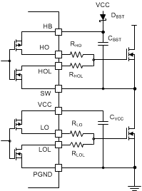 Figure 30. Drivers with Slew Rate Control
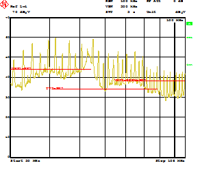 Figure 31. Conducted EMI Measurement, Without Slew Rate Control
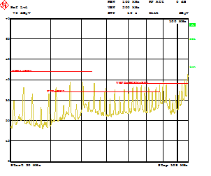 Figure 32. Conducted EMI Measurements, With Slew Rate Control
8.2.6.4 Frequency Dithering
Figure 33 shows the conducted emission test run on the LM5141EVM, without the Dither feature enabled. The first harmonic (peak measurement) is 48 dBµV, Figure 34 shows the conducted emissions test results with the Dither feature enabled. With the Dither featured enabled, the first harmonic (peak measurement) was lowered to 40 dBµV, an 8 dB reduction.
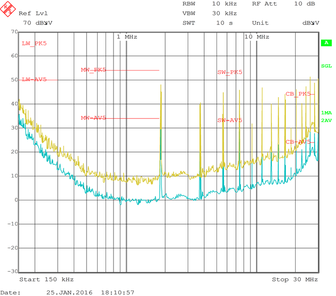 Figure 33. Measured Conducted EMI, Without Dither
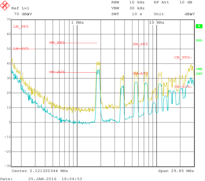 Figure 34. Measured Conducted EMI, With Dither
8.2.7 8.9 Control Loop
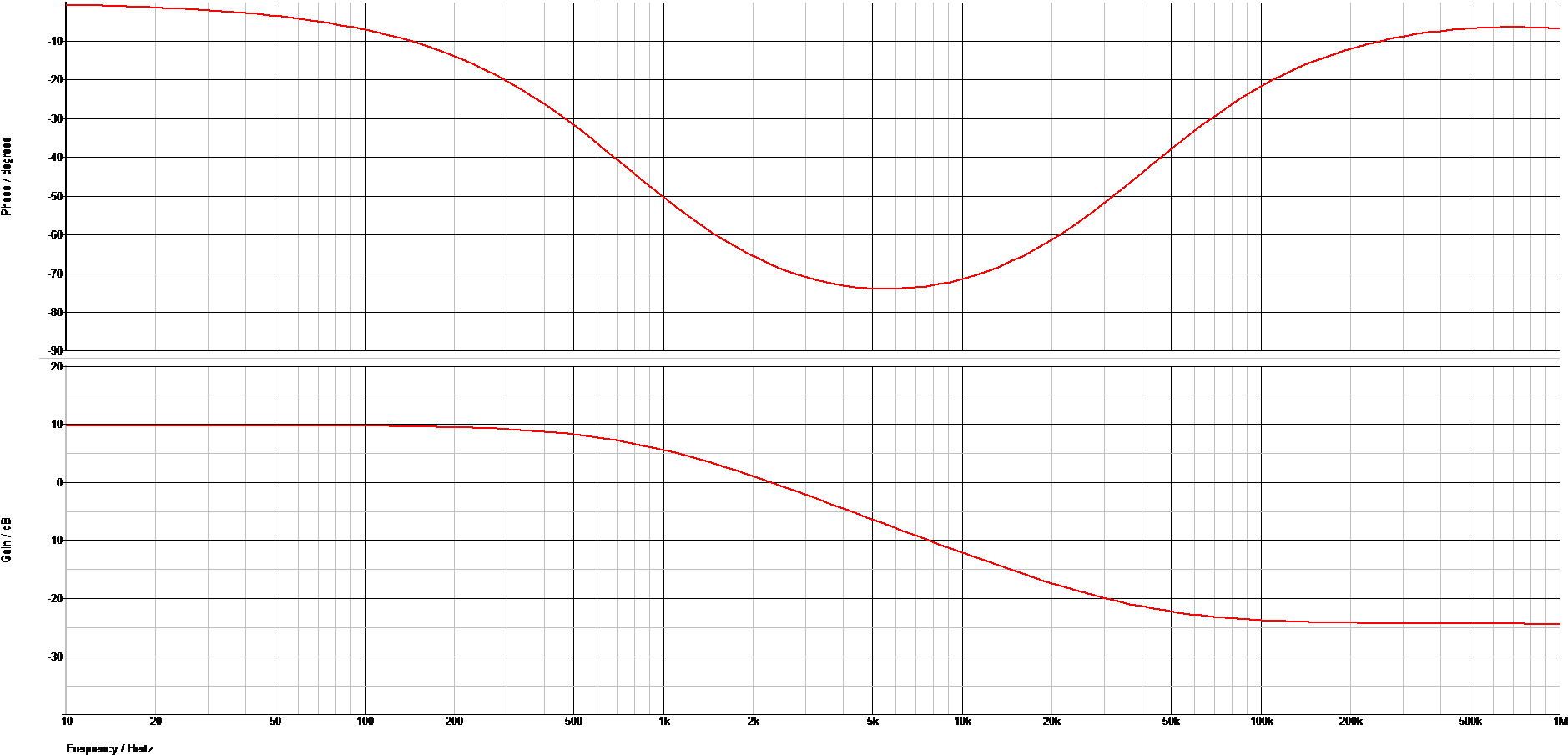
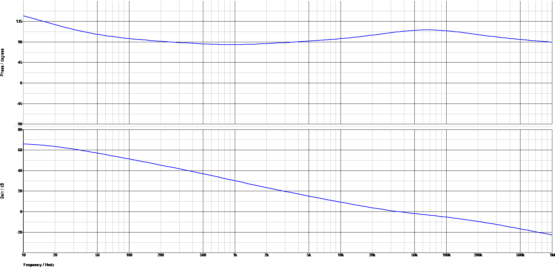
The open loop gain is defined as the product of modulator transfer function and feedback transfer function. When plotted on a dB scale, the open loop gain is shown as the sum of modulator gain and feedback gain.
DC modulator gain is:

The modulator gain plus power stage transfer function with an embedded current loop is show in Equation 50. The equation includes the sample gain at FSW /2 (ωn), which is caused by sampling effect of current mode control.
Because the loop cross over frequency is well below sample gain effects, Equation 50 can be simplified as one pole and a one zero system as shown in Equation 51.

RLOAD is the load resistance
RDCR is the dc resistance on the output inductor which is 8.1 mΩ
RSENSE is the current sense resistance which is 9 mΩ
8.2.7.1 Feedback Compensator
A type II compensator using an transconductance error amplifier (EA), Gm, is shown in Figure 35. The dominant pole of the EA open-loop gain is set by the EA output resistance, RAMP, and effective bandwidth-limiting capacitance, CO, as follows:

The EA high frequency pole is neglected in the above expression. The compensator transfer function from output voltage to COMP, including the gain contribution from the feedback resistor divider network is:


where

Which simplifies to:

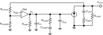 Figure 35. Transconductance Amplifier


Typically RCOMP << RAMP and CCOMP >> (CHF + CO) so the approximations are valid.
where
VREF is the feedback voltage reference (1.2 V)
Gm is the error amplifier gain transconductance (1200 µS)
RAMP is the error amplifier output impedance (2.5 MΩ)
The error amplifier compensation components create a pole at the origin, a zero, and a high frequency pole.
The procedure for choosing compensation components for a stable closed loop is:
- Select the desired open loop gain crossover frequency (fc); for this application 30 kHz was chosen
- Calculate the RCOMP resistor for the gain crossover frequency at 30 kHz
- Calculate the CCOMP capacitor value to create a zero that cancels the pole ωp ( ωp = 1/RLOAD × COUT)

The value selected for RCOMP is 22.6 kΩ.
where
RDCR = 0.0081 Ω

The value selected for CCOMP is 10nF.


