ZHCSIY8C October   2018  – June 2021 LM5143-Q1

PRODUCTION DATA  

  1. 特性
  2. 应用
  3. 说明
  4. Revision History
  5. 说明(续)
  6. Pin Configuration and Functions
    1. 6.1 Wettable Flanks
  7. Specifications
    1. 7.1 Absolute Maximum Ratings
    2. 7.2 ESD Ratings
    3. 7.3 Recommended Operating Conditions
    4. 7.4 Thermal Information
    5. 7.5 Electrical Characteristics
    6. 7.6 Switching Characteristics
    7. 7.7 Typical Characteristics
  8. Detailed Description
    1. 8.1 Overview
    2. 8.2 Functional Block Diagram
    3. 8.3 Feature Description
      1. 8.3.1  Input Voltage Range (VIN)
      2. 8.3.2  High-Voltage Bias Supply Regulator (VCC, VCCX, VDDA)
      3. 8.3.3  Enable (EN1, EN2)
      4. 8.3.4  Power Good Monitor (PG1, PG2)
      5. 8.3.5  Switching Frequency (RT)
      6. 8.3.6  Clock Synchronization (DEMB)
      7. 8.3.7  Synchronization Out (SYNCOUT)
      8. 8.3.8  Spread Spectrum Frequency Modulation (DITH)
      9. 8.3.9  Configurable Soft Start (SS1, SS2)
      10. 8.3.10 Output Voltage Setpoint (FB1, FB2)
      11. 8.3.11 Minimum Controllable On-Time
      12. 8.3.12 Error Amplifier and PWM Comparator (FB1, FB2, COMP1, COMP2)
      13. 8.3.13 Slope Compensation
      14. 8.3.14 Inductor Current Sense (CS1, VOUT1, CS2, VOUT2)
        1. 8.3.14.1 Shunt Current Sensing
        2. 8.3.14.2 Inductor DCR Current Sensing
      15. 8.3.15 Hiccup Mode Current Limiting (RES)
      16. 8.3.16 High-Side and Low-Side Gate Drivers (HO1/2, LO1/2, HOL1/2, LOL1/2)
      17. 8.3.17 Output Configurations (MODE, FB2)
        1. 8.3.17.1 Independent Dual-Output Operation
        2. 8.3.17.2 Single-Output Interleaved Operation
        3. 8.3.17.3 Single-Output Multiphase Operation
    4. 8.4 Device Functional Modes
      1. 8.4.1 Standby Modes
      2. 8.4.2 Diode Emulation Mode
      3. 8.4.3 Thermal Shutdown
  9. Application and Implementation
    1. 9.1 Application Information
      1. 9.1.1 Power Train Components
        1. 9.1.1.1 Buck Inductor
        2. 9.1.1.2 Output Capacitors
        3. 9.1.1.3 Input Capacitors
        4. 9.1.1.4 Power MOSFETs
        5. 9.1.1.5 EMI Filter
      2. 9.1.2 Error Amplifier and Compensation
    2. 9.2 Typical Applications
      1. 9.2.1 Design 1 – High Efficiency, Dual-Output Buck Regulator for Automotive Applications
        1. 9.2.1.1 Design Requirements
        2. 9.2.1.2 Detailed Design Procedure
          1. 9.2.1.2.1 Custom Design With WEBENCH® Tools
          2. 9.2.1.2.2 Custom Design With Excel Quickstart Tool
          3. 9.2.1.2.3 Inductor Calculation
          4. 9.2.1.2.4 Current-Sense Resistance
          5. 9.2.1.2.5 Output Capacitors
          6. 9.2.1.2.6 Input Capacitors
          7. 9.2.1.2.7 Compensation Components
        3. 9.2.1.3 Application Curves
      2. 9.2.2 Design 2 – Two-Phase, Single-Output Buck Regulator for Automotive ADAS Applications
        1. 9.2.2.1 Design Requirements
        2. 9.2.2.2 Detailed Design Procedures
        3. 9.2.2.3 Application Curves
  10. 10Power Supply Recommendations
  11. 11Layout
    1. 11.1 Layout Guidelines
      1. 11.1.1 Power Stage Layout
      2. 11.1.2 Gate-Drive Layout
      3. 11.1.3 PWM Controller Layout
      4. 11.1.4 Thermal Design and Layout
      5. 11.1.5 Ground Plane Design
    2. 11.2 Layout Example
  12. 12Device and Documentation Support
    1. 12.1 Device Support
      1. 12.1.1 第三方米6体育平台手机版_好二三四免责声明
      2. 12.1.2 Development Support
      3. 12.1.3 Custom Design With WEBENCH® Tools
    2. 12.2 Documentation Support
      1. 12.2.1 Related Documentation
        1. 12.2.1.1 PCB Layout Resources
        2. 12.2.1.2 Thermal Design Resources
    3. 12.3 接收文档更新通知
    4. 12.4 支持资源
    5. 12.5 Trademarks
    6. 12.6 Electrostatic Discharge Caution
    7. 12.7 Glossary
  13. 13Mechanical, Packaging, and Orderable Information

封装选项

机械数据 (封装 | 引脚)
散热焊盘机械数据 (封装 | 引脚)
订购信息

Output Voltage Setpoint (FB1, FB2)

The LM5143-Q1 outputs can be independently configured for one of the two fixed output voltages with no external feedback resistors, or adjusted to the desired voltage using an external resistor divider. VOUT1 or VOUT2 can be configured as a 3.3-V output by connecting the corresponding FB pin to VDDA, or a 5-V output by connecting FB to AGND. The FB1 and FB2 connections (either VDDA or GND) are detected during power up. The configuration settings are latched and cannot be changed until the LM5143-Q1 is powered down with the VCC voltage decreasing below its falling UVLO threshold, and then powered up again.

Alternatively, the output voltage can be set using external resistive dividers from the output to the relevant FB pin. The output voltage adjustment range is between 0.6 V and 55 V. The regulation threshold at FB is 0.6 V (VREF). Use Equation 5 to calculate the upper and lower feedback resistors, designated RFB1 and RFB2, respectively. See Figure 8-3.

Equation 5. GUID-AFECFD51-4009-47B9-9799-B49E20C3B226-low.gif

The recommended starting value for RFB2 is between 10 kΩ and 20 kΩ.
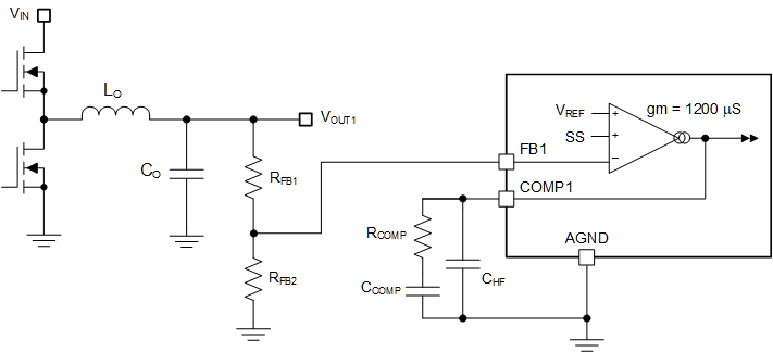
GUID-20210407-CA0I-J7CM-HDQS-FLHT0HRQ1LRH-low.gif Figure 8-3 Control Loop Error Amplifier

The Thevenin equivalent impedance of the resistive divider connected to the FB pin must be greater than 5 kΩ for the LM5143-Q1 to detect the divider and set the channel to the adjustable output mode.

Equation 6. GUID-54CD85E2-EE28-44A3-9E65-E407F63129DE-low.gif

If a low IQ mode is required, take care when selecting the external resistors. The extra current drawn from the external divider is added to the LM5143-Q1 ISTANDBY current (15 µA typical). The divider current reflected to VIN is divided down by the ratio of VOUT/VIN. For example, if VOUT is set to 5.55 V with RFB1 equal to 82.5 kΩ and RFB2 equal to 10 kΩ, use Equation 7 to calculate the input current from a 12-V input required to supply the current in the feedback resistors.

Equation 7. GUID-E6EAFB8F-BA34-4482-BC49-CC8B9AF4CDF3-low.gif
If one output is enabled and the other disabled, the VCC output is in regulation. The HB voltage of the disabled channel charges to VCC through the bootstrap diode. As a result, the HO driver bias current (approximately 1.5 µA) can increase the output voltage of the disabled channel to approximately 2.2 V. If this is not desired, add a load resistor (100 kΩ) to the output that is disabled to maintain a low-voltage OFF-state.