ZHCSIY8C October   2018  – June 2021 LM5143-Q1

PRODUCTION DATA  

  1. 特性
  2. 应用
  3. 说明
  4. Revision History
  5. 说明(续)
  6. Pin Configuration and Functions
    1. 6.1 Wettable Flanks
  7. Specifications
    1. 7.1 Absolute Maximum Ratings
    2. 7.2 ESD Ratings
    3. 7.3 Recommended Operating Conditions
    4. 7.4 Thermal Information
    5. 7.5 Electrical Characteristics
    6. 7.6 Switching Characteristics
    7. 7.7 Typical Characteristics
  8. Detailed Description
    1. 8.1 Overview
    2. 8.2 Functional Block Diagram
    3. 8.3 Feature Description
      1. 8.3.1  Input Voltage Range (VIN)
      2. 8.3.2  High-Voltage Bias Supply Regulator (VCC, VCCX, VDDA)
      3. 8.3.3  Enable (EN1, EN2)
      4. 8.3.4  Power Good Monitor (PG1, PG2)
      5. 8.3.5  Switching Frequency (RT)
      6. 8.3.6  Clock Synchronization (DEMB)
      7. 8.3.7  Synchronization Out (SYNCOUT)
      8. 8.3.8  Spread Spectrum Frequency Modulation (DITH)
      9. 8.3.9  Configurable Soft Start (SS1, SS2)
      10. 8.3.10 Output Voltage Setpoint (FB1, FB2)
      11. 8.3.11 Minimum Controllable On-Time
      12. 8.3.12 Error Amplifier and PWM Comparator (FB1, FB2, COMP1, COMP2)
      13. 8.3.13 Slope Compensation
      14. 8.3.14 Inductor Current Sense (CS1, VOUT1, CS2, VOUT2)
        1. 8.3.14.1 Shunt Current Sensing
        2. 8.3.14.2 Inductor DCR Current Sensing
      15. 8.3.15 Hiccup Mode Current Limiting (RES)
      16. 8.3.16 High-Side and Low-Side Gate Drivers (HO1/2, LO1/2, HOL1/2, LOL1/2)
      17. 8.3.17 Output Configurations (MODE, FB2)
        1. 8.3.17.1 Independent Dual-Output Operation
        2. 8.3.17.2 Single-Output Interleaved Operation
        3. 8.3.17.3 Single-Output Multiphase Operation
    4. 8.4 Device Functional Modes
      1. 8.4.1 Standby Modes
      2. 8.4.2 Diode Emulation Mode
      3. 8.4.3 Thermal Shutdown
  9. Application and Implementation
    1. 9.1 Application Information
      1. 9.1.1 Power Train Components
        1. 9.1.1.1 Buck Inductor
        2. 9.1.1.2 Output Capacitors
        3. 9.1.1.3 Input Capacitors
        4. 9.1.1.4 Power MOSFETs
        5. 9.1.1.5 EMI Filter
      2. 9.1.2 Error Amplifier and Compensation
    2. 9.2 Typical Applications
      1. 9.2.1 Design 1 – High Efficiency, Dual-Output Buck Regulator for Automotive Applications
        1. 9.2.1.1 Design Requirements
        2. 9.2.1.2 Detailed Design Procedure
          1. 9.2.1.2.1 Custom Design With WEBENCH® Tools
          2. 9.2.1.2.2 Custom Design With Excel Quickstart Tool
          3. 9.2.1.2.3 Inductor Calculation
          4. 9.2.1.2.4 Current-Sense Resistance
          5. 9.2.1.2.5 Output Capacitors
          6. 9.2.1.2.6 Input Capacitors
          7. 9.2.1.2.7 Compensation Components
        3. 9.2.1.3 Application Curves
      2. 9.2.2 Design 2 – Two-Phase, Single-Output Buck Regulator for Automotive ADAS Applications
        1. 9.2.2.1 Design Requirements
        2. 9.2.2.2 Detailed Design Procedures
        3. 9.2.2.3 Application Curves
  10. 10Power Supply Recommendations
  11. 11Layout
    1. 11.1 Layout Guidelines
      1. 11.1.1 Power Stage Layout
      2. 11.1.2 Gate-Drive Layout
      3. 11.1.3 PWM Controller Layout
      4. 11.1.4 Thermal Design and Layout
      5. 11.1.5 Ground Plane Design
    2. 11.2 Layout Example
  12. 12Device and Documentation Support
    1. 12.1 Device Support
      1. 12.1.1 第三方米6体育平台手机版_好二三四免责声明
      2. 12.1.2 Development Support
      3. 12.1.3 Custom Design With WEBENCH® Tools
    2. 12.2 Documentation Support
      1. 12.2.1 Related Documentation
        1. 12.2.1.1 PCB Layout Resources
        2. 12.2.1.2 Thermal Design Resources
    3. 12.3 接收文档更新通知
    4. 12.4 支持资源
    5. 12.5 Trademarks
    6. 12.6 Electrostatic Discharge Caution
    7. 12.7 Glossary
  13. 13Mechanical, Packaging, and Orderable Information

封装选项

机械数据 (封装 | 引脚)
散热焊盘机械数据 (封装 | 引脚)
订购信息

Design 1 – High Efficiency, Dual-Output Buck Regulator for Automotive Applications

Figure 9-4 shows the schematic diagram of a dual-output synchronous buck regulator with output voltages setpoints of 3.3 V and 5 V and a rated load current of 7 A for each output. In this example, the target half-load and full-load efficiencies are 91% and 90%, respectively, based on a nominal input voltage of 12 V that ranges from 3.5 V to 36 V. The switching frequency is set at 2.1 MHz by resistor RRT. The 5-V output is connected to VCCX to reduce IC bias power dissipation and improve efficiency.
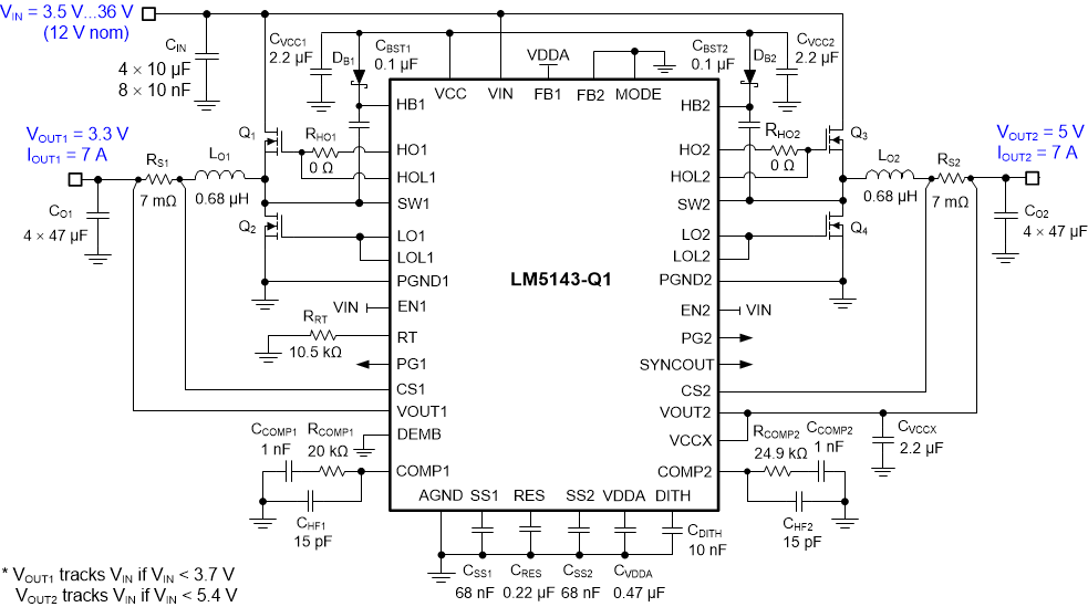
GUID-97EFDAD3-26CE-455B-BF92-E0185B28D7F8-low.gif Figure 9-4 Application Circuit 1 With LM5143-Q1 Buck Regulator at 2.1 MHz
Note:

This and subsequent design examples are provided herein to showcase the LM5143-Q1 controller in several different applications. Depending on the source impedance of the input supply bus, an electrolytic capacitor can be required at the input to ensure stability, particularly at low input voltage and high output current operating conditions. See Section 10 for more details.