ZHCSIY8C October 2018 – June 2021 LM5143-Q1
PRODUCTION DATA
- 1 特性
- 2 应用
- 3 说明
- 4 Revision History
- 5 说明(续)
- 6 Pin Configuration and Functions
- 7 Specifications
-
8 Detailed Description
- 8.1 Overview
- 8.2 Functional Block Diagram
- 8.3
Feature Description
- 8.3.1 Input Voltage Range (VIN)
- 8.3.2 High-Voltage Bias Supply Regulator (VCC, VCCX, VDDA)
- 8.3.3 Enable (EN1, EN2)
- 8.3.4 Power Good Monitor (PG1, PG2)
- 8.3.5 Switching Frequency (RT)
- 8.3.6 Clock Synchronization (DEMB)
- 8.3.7 Synchronization Out (SYNCOUT)
- 8.3.8 Spread Spectrum Frequency Modulation (DITH)
- 8.3.9 Configurable Soft Start (SS1, SS2)
- 8.3.10 Output Voltage Setpoint (FB1, FB2)
- 8.3.11 Minimum Controllable On-Time
- 8.3.12 Error Amplifier and PWM Comparator (FB1, FB2, COMP1, COMP2)
- 8.3.13 Slope Compensation
- 8.3.14 Inductor Current Sense (CS1, VOUT1, CS2, VOUT2)
- 8.3.15 Hiccup Mode Current Limiting (RES)
- 8.3.16 High-Side and Low-Side Gate Drivers (HO1/2, LO1/2, HOL1/2, LOL1/2)
- 8.3.17 Output Configurations (MODE, FB2)
- 8.4 Device Functional Modes
-
9 Application and Implementation
- 9.1 Application Information
- 9.2 Typical Applications
- 10Power Supply Recommendations
- 11Layout
- 12Device and Documentation Support
- 13Mechanical, Packaging, and Orderable Information
11.1 Layout Guidelines
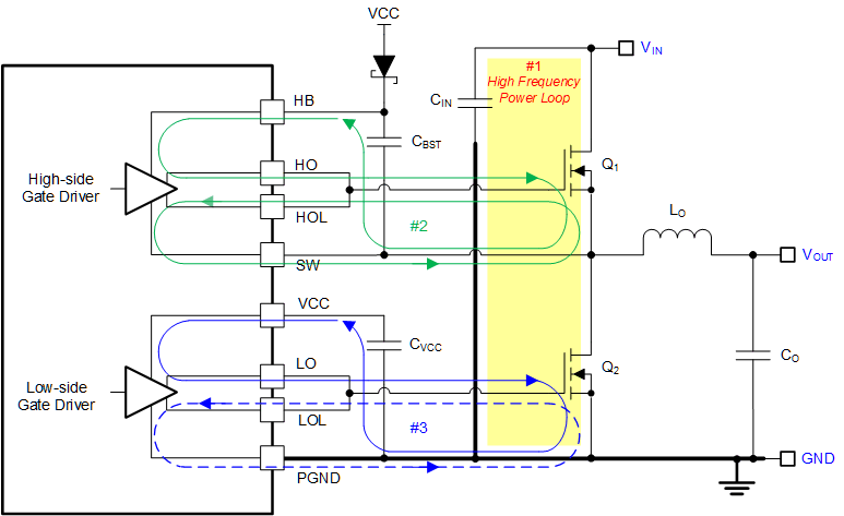
Proper PCB design and layout is important in a high-current, fast-switching circuits (with high current and voltage slew rates) to achieve a robust and reliable design. As expected, certain issues must be considered before designing a PCB layout using the LM5143-Q1. The high-frequency power loop of a buck regulator power stage is denoted by loop 1 in the shaded area of Figure 11-1. The topological architecture of a buck regulator means that particularly high di/dt current flows in the components of loop 1, and it becomes mandatory to reduce the parasitic inductance of this loop by minimizing its effective loop area. Also important are the gate drive loops of the low-side and high-side MOSFETs, denoted by 2 and 3, respectively, in Figure 11-1.
 Figure 11-1 DC/DC Regulator Ground System With
Power Stage and Gate Drive Circuit Switching Loops