ZHCSIY8C October 2018 – June 2021 LM5143-Q1
PRODUCTION DATA
- 1 特性
- 2 应用
- 3 说明
- 4 Revision History
- 5 说明(续)
- 6 Pin Configuration and Functions
- 7 Specifications
-
8 Detailed Description
- 8.1 Overview
- 8.2 Functional Block Diagram
- 8.3
Feature Description
- 8.3.1 Input Voltage Range (VIN)
- 8.3.2 High-Voltage Bias Supply Regulator (VCC, VCCX, VDDA)
- 8.3.3 Enable (EN1, EN2)
- 8.3.4 Power Good Monitor (PG1, PG2)
- 8.3.5 Switching Frequency (RT)
- 8.3.6 Clock Synchronization (DEMB)
- 8.3.7 Synchronization Out (SYNCOUT)
- 8.3.8 Spread Spectrum Frequency Modulation (DITH)
- 8.3.9 Configurable Soft Start (SS1, SS2)
- 8.3.10 Output Voltage Setpoint (FB1, FB2)
- 8.3.11 Minimum Controllable On-Time
- 8.3.12 Error Amplifier and PWM Comparator (FB1, FB2, COMP1, COMP2)
- 8.3.13 Slope Compensation
- 8.3.14 Inductor Current Sense (CS1, VOUT1, CS2, VOUT2)
- 8.3.15 Hiccup Mode Current Limiting (RES)
- 8.3.16 High-Side and Low-Side Gate Drivers (HO1/2, LO1/2, HOL1/2, LOL1/2)
- 8.3.17 Output Configurations (MODE, FB2)
- 8.4 Device Functional Modes
-
9 Application and Implementation
- 9.1 Application Information
- 9.2 Typical Applications
- 10Power Supply Recommendations
- 11Layout
- 12Device and Documentation Support
- 13Mechanical, Packaging, and Orderable Information
11.2 Layout Example
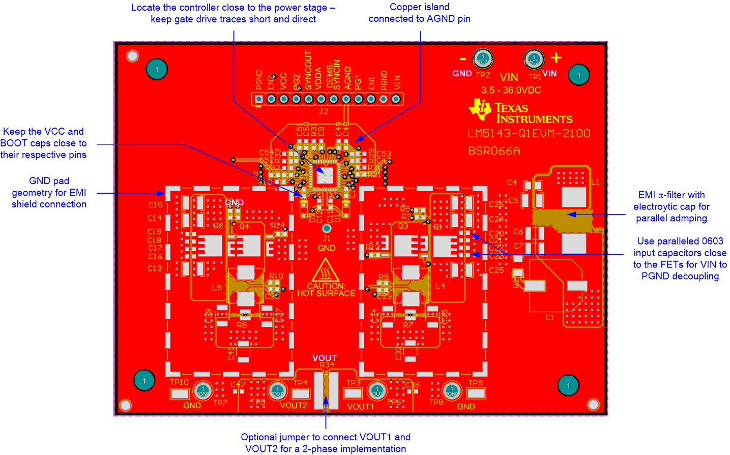
Based on the LM5143-Q1EVM-2100 design, Figure 11-2 shows a single-sided layout of a dual-output synchronous buck regulator. Each power stage is surrounded by a GND pad geometry to connect an EMI shield if needed. The design uses layer 2 of the PCB as a power-loop return path directly underneath the top layer to create a low-area switching power loop of approximately 2 mm². This loop area, and hence parasitic inductance, must be as small as possible to minimize EMI as well as switch-node voltage overshoot and ringing. Refer to the LM5143-Q1EVM-2100 Evaluation Module User's Guide for more detail.
 Figure 11-2 PCB Top Layer
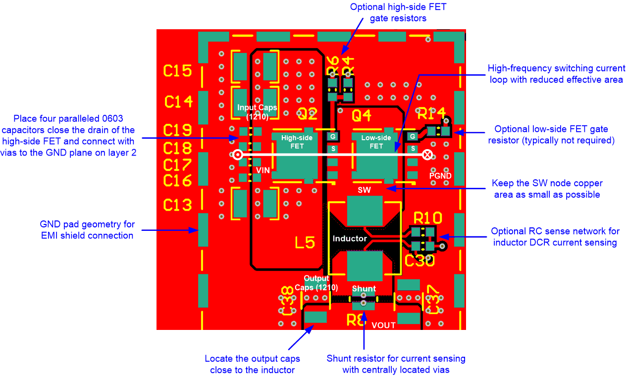
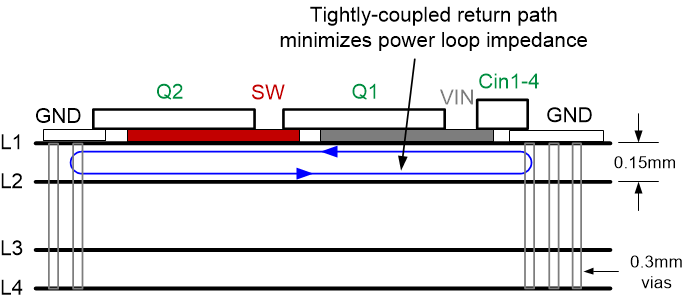
As shown in Figure 11-3, the high-frequency power loop current of one channel flows through MOSFETs Q2 and Q4, through the power ground plane on layer 2, and back to VIN through the 0603 ceramic capacitors C16 through C19. The currents flowing in opposing directions in the vertical loop configuration provide field self-cancellation, reducing parasitic inductance. Figure 11-4 shows a side view to illustrate the concept of creating a low-profile, self-canceling loop in a multilayer PCB structure. The layer-2 GND plane layer, shown in Figure 11-3, provides a tightly-coupled current return path directly under the MOSFETs to the source terminals of Q2.
Four 10-nF input capacitors with small 0402 or 0603 case size are placed in parallel very close to the drain of each high-side MOSFET. The low equivalent series inductance (ESL) and high self-resonant frequency (SRF) of the small footprint capacitors yield excellent high-frequency performance. The negative terminals of these capacitors are connected to the layer-2 GND plane with multiple 12-mil (0.3-mm) diameter vias, further minimizing parasitic loop inductance.
Additional steps used in this layout example include:
- Keep the SW connection from the power MOSFETs to the inductor (for each channel) at minimum copper area to reduce radiated EMI.
- Locate the controller close to the gate terminals of the MOSFETs such that the gate drive traces are routed short and direct.
- Create an analog ground plane near the controller for sensitive analog components. The analog ground plane for AGND and power ground planes for PGND1 and PGND2 must be connected at a single point directly under the IC – at the die attach pad (DAP).
 Figure 11-3 Power Stage Component Layout