ZHCSIY8C October 2018 – June 2021 LM5143-Q1
PRODUCTION DATA
- 1 特性
- 2 应用
- 3 说明
- 4 Revision History
- 5 说明(续)
- 6 Pin Configuration and Functions
- 7 Specifications
-
8 Detailed Description
- 8.1 Overview
- 8.2 Functional Block Diagram
- 8.3
Feature Description
- 8.3.1 Input Voltage Range (VIN)
- 8.3.2 High-Voltage Bias Supply Regulator (VCC, VCCX, VDDA)
- 8.3.3 Enable (EN1, EN2)
- 8.3.4 Power Good Monitor (PG1, PG2)
- 8.3.5 Switching Frequency (RT)
- 8.3.6 Clock Synchronization (DEMB)
- 8.3.7 Synchronization Out (SYNCOUT)
- 8.3.8 Spread Spectrum Frequency Modulation (DITH)
- 8.3.9 Configurable Soft Start (SS1, SS2)
- 8.3.10 Output Voltage Setpoint (FB1, FB2)
- 8.3.11 Minimum Controllable On-Time
- 8.3.12 Error Amplifier and PWM Comparator (FB1, FB2, COMP1, COMP2)
- 8.3.13 Slope Compensation
- 8.3.14 Inductor Current Sense (CS1, VOUT1, CS2, VOUT2)
- 8.3.15 Hiccup Mode Current Limiting (RES)
- 8.3.16 High-Side and Low-Side Gate Drivers (HO1/2, LO1/2, HOL1/2, LOL1/2)
- 8.3.17 Output Configurations (MODE, FB2)
- 8.4 Device Functional Modes
-
9 Application and Implementation
- 9.1 Application Information
- 9.2 Typical Applications
- 10Power Supply Recommendations
- 11Layout
- 12Device and Documentation Support
- 13Mechanical, Packaging, and Orderable Information
8.3.17.3 Single-Output Multiphase Operation
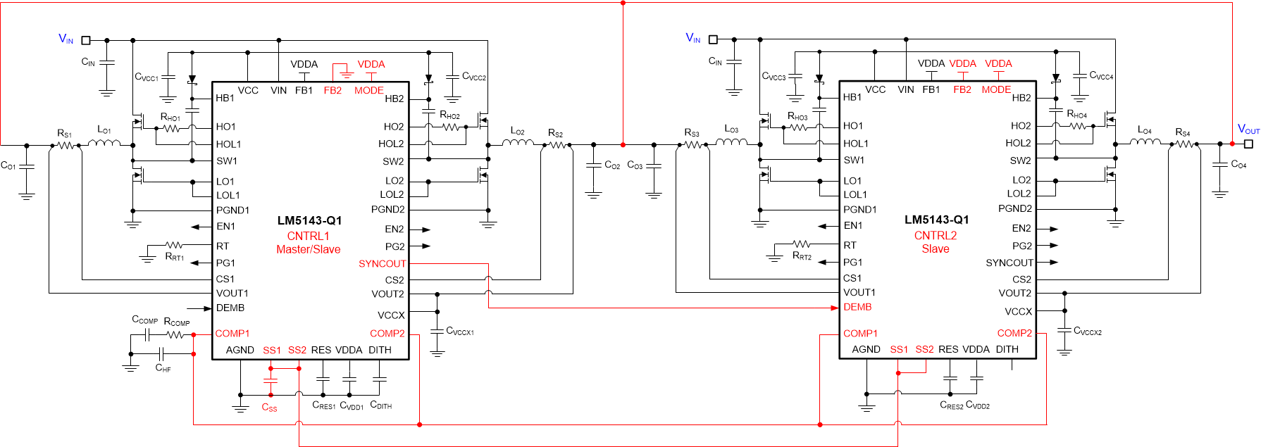
To configure the LM5143-Q1 for multiphase operation (three or four phases), two LM5143-Q1 controllers are required. See Figure 8-10. Configure the first controller (CNTRL1) as a master and the second controller (CNTRL2) as a slave. To configure the second controller as a slave, connect the MODE and FB2 pins to VDDA. This disables both feedback error amplifiers of the slave controller, placing them in a high-impedance state. Connect COMP1 and COMP2 of the master and slave together. Connect SS1 and SS2 of the master and slave together. Connect SYNCOUT of the master to DEMB (SYNCIN) of the slave. The SYNCOUT of the master controller is 90° out-of-phase and facilitates interleaved operation. RT is not used for the oscillator when the LM5143-Q1 is in slave mode but instead used for slope compensation. Therefore, select the RT resistance to be the same as that of the master. The oscillator is derived from the master controller. FPWM or DEM mode for the slave is set by connecting its FB1 to VDDA or GND. FPWM or DEM mode of the master controller is set by its DEMB pin. See Table 8-3.
The LM5143-Q1 in single-output multiphase operation does not support phase shedding when the output voltage is set between 0.6 V to 1.5 V.
See the Benefits of a Multiphase Buck Converter White Paper and Multiphase Buck Design From Start to Finish Application Report for more information.
| MODE | FB1 (SLAVE) | FB2 (SLAVE) | DEM or FPWM (SLAVE) |
|---|---|---|---|
| VDDA | GND | VDDA | DEM |
| VDDA | VDDA | VDDA | FPWM |
 Figure 8-10 Multiphase Regulator Schematic Configured for Single-Output Interleaved Operation