ZHCSGB0B November 2017 – November 2020 LM5145
PRODUCTION DATA
- 1 特性
- 2 应用
- 3 说明
- 4 Revision History
- 5 Description (continued)
- 6 Pin Configuration and Functions
- 7 Specifications
-
8 Detailed Description
- 8.1 Overview
- 8.2 Functional Block Diagram
- 8.3
Feature Description
- 8.3.1 Input Range (VIN)
- 8.3.2 Output Voltage Setpoint and Accuracy (FB)
- 8.3.3 High-Voltage Bias Supply Regulator (VCC)
- 8.3.4 Precision Enable (EN/UVLO)
- 8.3.5 Power Good Monitor (PGOOD)
- 8.3.6 Switching Frequency (RT, SYNCIN)
- 8.3.7 Configurable Soft Start (SS/TRK)
- 8.3.8 Voltage-Mode Control (COMP)
- 8.3.9 Gate Drivers (LO, HO)
- 8.3.10 Current Sensing and Overcurrent Protection (ILIM)
- 8.3.11 OCP Duty Cycle Limiter
- 8.4 Device Functional Modes
-
9 Application and Implementation
- 9.1 Application Information
- 9.2
Typical Applications
- 9.2.1 Design 1 – 20-A High-Efficiency Synchronous Buck Regulator for Telecom Power Applications
- 9.2.2 Design 2 – High Density, 12-V, 10-A Rail With LDO Low-Noise Auxiliary Output for RF Power Applications
- 9.2.3 Design 3 – 150-W, Regulated 24-V Rail for Commercial Drone Applications With Output Voltage Tracking Feature
- 9.2.4 Design 4 – Powering a Multicore DSP From a 24-V or 48-V Rail
- 10Power Supply Recommendations
- 11Layout
- 12Device and Documentation Support
- 13Mechanical, Packaging, and Orderable Information
8.3.1 Input Range (VIN)
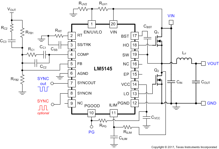
The LM5145 operational input voltage range is from 6 V to 75 V. The device is intended for step-down conversions from 12-V, 24-V, 48-V, 60-V, and 72-V unregulated, semiregulated, and fully-regulated supply rails. The application circuit in Figure 8-1 shows all the necessary components to implement an LM5145-based wide-VIN step-down regulator using a single supply. The LM5145 uses an internal LDO subregulator to provide a 7.5-V VCC bias rail for the gate drive and control circuits (assuming the input voltage is higher than 7.5 V plus the necessary subregulator dropout specification).
 Figure 8-1 Schematic Diagram for VIN Operating Range of 6 V to 75 V
In high voltage applications, take extra care to ensure the VIN pin does not exceed the absolute maximum voltage rating of 105 V during line or load transient events. Voltage ringing on the VIN pin that exceeds the Section 7.1 can damage the IC. Use high-quality ceramic input capacitors to minimize ringing. An RC filter from the input rail to the VIN pin (for example, 4.7 Ω and 0.1 µF) provides supplementary filtering at the VIN pin.