ZHCSMX3C December 2020 – February 2023 LM5149-Q1
PRODUCTION DATA
- 1 特性
- 2 应用
- 3 说明
- 4 Revision History
- 5 说明(续)
- 6 Pin Configuration and Functions
- 7 Specifications
-
8 Detailed Description
- 8.1 Overview
- 8.2 Functional Block Diagram
- 8.3
Feature Description
- 8.3.1 Input Voltage Range (VIN)
- 8.3.2 High-Voltage Bias Supply Regulator (VCC, VCCX, VDDA)
- 8.3.3 Precision Enable (EN)
- 8.3.4 Power-Good Monitor (PG)
- 8.3.5 Switching Frequency (RT)
- 8.3.6 Active EMI Filter
- 8.3.7 Dual Random Spread Spectrum (DRSS)
- 8.3.8 Soft Start
- 8.3.9 Output Voltage Setpoint (FB)
- 8.3.10 Minimum Controllable On Time
- 8.3.11 Error Amplifier and PWM Comparator (FB, EXTCOMP)
- 8.3.12 Slope Compensation
- 8.3.13 Inductor Current Sense (ISNS+, VOUT)
- 8.3.14 Hiccup Mode Current Limiting
- 8.3.15 High-Side and Low-Side Gate Drivers (HO, LO)
- 8.3.16 Output Configurations (CNFG)
- 8.3.17 Single-Output Dual-Phase Operation
- 8.4 Device Functional Modes
-
9 Application and Implementation
- 9.1 Application Information
- 9.2
Typical Applications
- 9.2.1
Design 1 – High-Efficiency 2.1-MHz Synchronous
Buck Regulator
- 9.2.1.1 Design Requirements
- 9.2.1.2
Detailed Design Procedure
- 9.2.1.2.1 Custom Design With WEBENCH® Tools
- 9.2.1.2.2 Custom Design With Excel Quickstart Tool
- 9.2.1.2.3 Buck Inductor
- 9.2.1.2.4 Current-Sense Resistance
- 9.2.1.2.5 Output Capacitors
- 9.2.1.2.6 Input Capacitors
- 9.2.1.2.7 Frequency Set Resistor
- 9.2.1.2.8 Feedback Resistors
- 9.2.1.2.9 Compensation Components
- 9.2.1.2.10 Active EMI Components
- 9.2.1.3 Application Curves
- 9.2.2 Design 2 – High Efficiency 48-V to 12-V 400-kHz Synchronous Buck Regulator
- 9.2.3 Design 3 – High Efficiency 440-kHz Synchronous Buck Regulator
- 9.2.4 Design 4 – Dual-Phase 400-kHz 20-A Synchronous Buck Regulator
- 9.2.1
Design 1 – High-Efficiency 2.1-MHz Synchronous
Buck Regulator
- 9.3 Power Supply Recommendations
- 9.4 Layout
- 10Device and Documentation Support
- 11Mechanical, Packaging, and Orderable Information
8.3.7 Dual Random Spread Spectrum (DRSS)
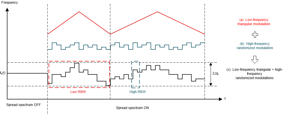
The LM5149-Q1 provides a digital spread spectrum, which reduces the EMI of the power supply over a wide frequency range. DRSS combines a low-frequency triangular modulation profile with a high frequency cycle-by-cycle random modulation profile. The low-frequency triangular modulation improves performance in lower radio-frequency bands, while the high-frequency random modulation improves performance in higher radio frequency bands.
Spread spectrum works by converting a narrowband signal into a wideband signal that spreads the energy over multiple frequencies. Because industry standards require different EMI receiver resolution bandwidth (RBW) settings for different frequency bands, the RBW has an impact on the spread spectrum performance. DRSS is able to simultaneously improve the EMI performance in the low and high RBWs with its low-frequency triangular modulation profile and high frequency cycle-by-cycle random modulation, respectively. DRSS can reduce conducted emissions by 15 dBμV in the CISPR 25 low-frequency band (150 kHz to 30 MHz) and 5 dBμV in the high-frequency band (30 MHz to 108 MHz).
To enable DRSS, connect either a 41.2-kΩ or 71.5-kΩ resistor from CNFG to AGND. DRSS is disabled when an external clock is applied to the PFM/SYNC pin.
 Figure 8-4 Dual Random Spread Spectrum
Implementation