ZHCSGU1C September 2017 – October 2021 LM5150-Q1
PRODUCTION DATA
- 1 特性
- 2 应用
- 3 说明
- 4 Revision History
- 5 Device Comparison Table
- 6 Pin Configuration and Functions
- 7 Specifications
-
8 Detailed Description
- 8.1 Overview
- 8.2 Functional Block Diagram
- 8.3
Feature Description
- 8.3.1 Enable (EN Pin)
- 8.3.2 High Voltage VCC Regulator (PVCC, AVCC Pin)
- 8.3.3 Power-On Voltage Selection (VSET Pin)
- 8.3.4 Switching Frequency (RT Pin)
- 8.3.5 Clock Synchronization (SYNC Pin in SS Configuration)
- 8.3.6 Current Sense, Slope Compensation, and PWM (CS Pin)
- 8.3.7 Current Limit (CS Pin)
- 8.3.8 Feedback and Error Amplifier (COMP Pin)
- 8.3.9 Automatic Wake-Up and Standby
- 8.3.10 Boost Status Indicator (STATUS Pin)
- 8.3.11 Maximum Duty Cycle Limit, Minimum Input Supply Voltage
- 8.3.12 MOSFET Driver (LO Pin)
- 8.3.13 Thermal Shutdown
- 8.4 Device Functional Modes
-
9 Application and Implementation
- 9.1 Application Information
- 9.2
Typical Application
- 9.2.1 Design Requirements
- 9.2.2
Detailed Design Procedure
- 9.2.2.1 Custom Design With WEBENCH® Tools
- 9.2.2.2 RSET Resistor
- 9.2.2.3 RT Resistor
- 9.2.2.4 Inductor Selection (LM)
- 9.2.2.5 Current Sense (RS)
- 9.2.2.6 Slope Compensation Ramp (RSL)
- 9.2.2.7 Output Capacitor (COUT)
- 9.2.2.8 Loop Compensation Component Selection and Maximum ESR
- 9.2.2.9 PVCC Capacitor, AVCC Capacitor, and AVCC Resistor
- 9.2.2.10 VOUT Filter (CVOUT, RVOUT)
- 9.2.2.11 Input Capacitor
- 9.2.2.12 MOSFET Selection
- 9.2.2.13 Diode Selection
- 9.2.2.14 Efficiency Estimation
- 9.2.3 Application Curves
- 9.3 System Examples
- 10Power Supply Recommendations
- 11Layout
- 12Device and Documentation Support
- 13Mechanical, Packaging, and Orderable Information
8.3.9 Automatic Wake-Up and Standby
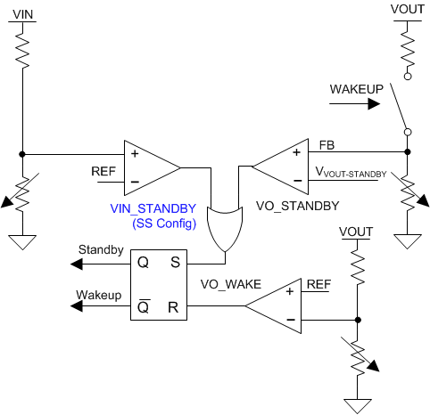
The LM5150-Q1 wakes up when VVOUT drops below the VOUT wake-up threshold. The device goes into standby when VVOUT rises above the VOUT standby threshold in EC or SS configuration or when VVIN rises above the VIN standby threshold in SS configuration. The VOUT wake-up threshold is typically 3% higher than the VOUT regulation target. The STATUS output is released in 3 µs (with a 50-kΩ pullup resistor to 5 V) after the wake-up event. The LO driver is enabled 6 µs after the STATUS output starts rising.
 Figure 8-3 Automatic Wake-Up and Standby Control
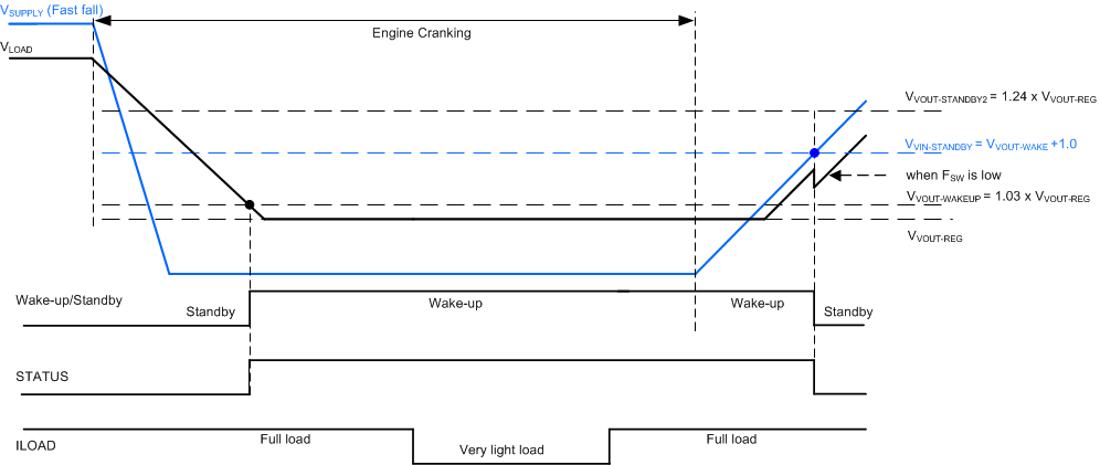
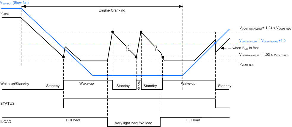
In SS configuration, the VOUT standby threshold is typically 24% higher than the VOUT regulation target. The VIN standby threshold is typically 1 V higher than the VOUT wake-up threshold in SS configuration. To prevent chatter, the forward voltage drop of diode D1 must be less than 0.95 V. See Figure 8-7.
 Figure 8-4 Automatic Wake-Up and Standby Operation in the SS Configuration (With Fast VSUPPLY Fall and Slow Switching)
 Figure 8-5 Automatic Wake-Up and Standby Operation in the SS Configuration (With Slow VSUPPLY Fall and Fast Switching)
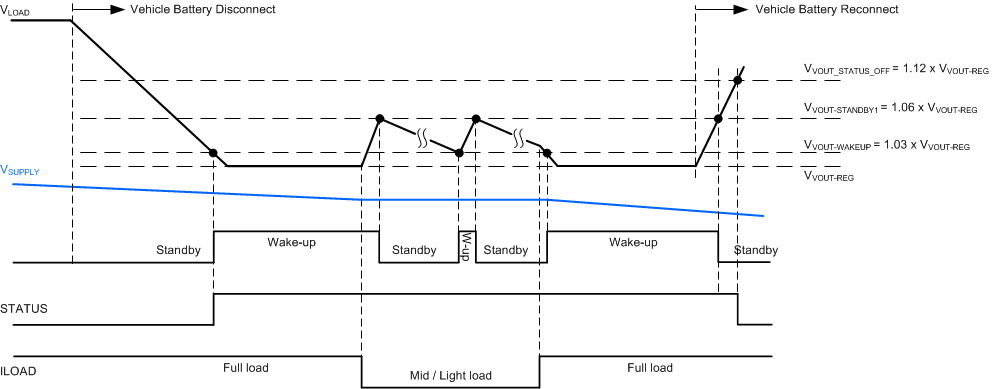
In EC configuration, the VOUT standby threshold is typically 6% higher than the VOUT regulation target. Because of the minimum duty cycle limit (see Section 8.4.3.2), the LM5150-Q1 alternates between the wake-up and the low IQ standby modes at medium or light load. See Figure 8-8.
 Figure 8-6 Automatic Wake-Up and Standby Operation in EC Configuration
To minimize output undershoot when waking up, the LM5150-Q1 boosts the VOUT regulation target during the first 128 cycles after the wake-up event. The regulation target becomes 3% higher than the original regulation target for 64 cycles, 2% higher for the next 32 cycles and 1% higher for the final 32 cycles. The VOUT pin voltage can rise up above the VOUT standby threshold even if switching stops at the VOUT standby threshold because the energy stored in the inductor transfers to the output capacitor when switching stops. See Section 8.4 for more information about the automatic wake-up and standby operation.