ZHCSHU0C March 2018 – October 2021 LM51501-Q1
PRODUCTION DATA
- 1 特性
- 2 应用
- 3 说明
- 4 Revision History
- 5 Device Comparison Table
- 6 Pin Configuration and Functions
- 7 Specifications
-
8 Detailed Description
- 8.1 Overview
- 8.2 Functional Block Diagram
- 8.3
Feature Description
- 8.3.1 Enable (EN Pin)
- 8.3.2 High Voltage VCC Regulator (PVCC, AVCC Pin)
- 8.3.3 Power-On Voltage Selection (VSET Pin)
- 8.3.4 Switching Frequency (RT Pin)
- 8.3.5 Clock Synchronization (SYNC Pin in SS Configuration)
- 8.3.6 Current Sense, Slope Compensation, and PWM (CS Pin)
- 8.3.7 Current Limit (CS Pin)
- 8.3.8 Feedback and Error Amplifier (COMP Pin)
- 8.3.9 Automatic Wake-Up and Standby
- 8.3.10 Boost Status Indicator (STATUS Pin)
- 8.3.11 Maximum Duty Cycle Limit and Minimum Input Supply Voltage
- 8.3.12 MOSFET Driver (LO Pin)
- 8.3.13 Thermal Shutdown
- 8.4 Device Functional Modes
-
9 Application and Implementation
- 9.1 Application Information
- 9.2
Typical Application
- 9.2.1 Design Requirements
- 9.2.2
Detailed Design Procedure
- 9.2.2.1 Custom Design With WEBENCH® Tools
- 9.2.2.2 RSET Resistor
- 9.2.2.3 RT Resistor
- 9.2.2.4 Inductor Selection (LM)
- 9.2.2.5 Current Sense (RS)
- 9.2.2.6 Slope Compensation Ramp (RSL)
- 9.2.2.7 Output Capacitor (COUT)
- 9.2.2.8 Loop Compensation Component Selection and Maximum ESR
- 9.2.2.9 PVCC Capacitor, AVCC Capacitor, and AVCC Resistor
- 9.2.2.10 VOUT Filter (CVOUT, RVOUT)
- 9.2.2.11 Input Capacitor
- 9.2.2.12 MOSFET Selection
- 9.2.2.13 Diode Selection
- 9.2.2.14 Efficiency Estimation
- 9.2.3 Application Curves
- 9.3 System Examples
- 10Power Supply Recommendations
- 11Layout
- 12Device and Documentation Support
- 13Mechanical, Packaging, and Orderable Information
8.3.3 Power-On Voltage Selection (VSET Pin)
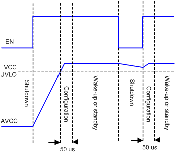
During initial power on, the VOUT regulation target and the configuration are configured by a resistor connected between the VSET and the AGND pins. The configuration starts when the EN pin voltage is greater than 2 V and the AVCC voltage crosses the AVCC UVLO threshold, which typically requires 50 µs to finish. To reset and reconfigure, the EN should be toggled below 1 V or the AVCC/VOUT must be fully discharged.
 Figure 8-1 Power-On Voltage Selection
The VOUT regulation target can be programmed to 6.0 V, 6.5 V, 9.5 V, or 11.5 V with the appropriate resistor with 5% tolerance. The configuration can be selected as either SS or EC configuration. The LM51501-Q1 will not switch during the 50-µs configuration time.
| CONFIGURATION | EMERGENCY-CALL | START-STOP | ||||||
|---|---|---|---|---|---|---|---|---|
| VOUT regulation target | 6.0 V | 6.5 V | 9.5 V | 11.5 V | 6.0 V | 6.5 V | 9.5 V | 11.5 V |
| RSET [Ω] | 90.9k | 71.5k | 54.9k | 41.2k | 29.4k | 19.1k | 9.53k | Ground |