ZHCSPX4A February 2022 – April 2022 LM5152-Q1 , LM51521-Q1
PRODUCTION DATA
- 1 特性
- 2 应用
- 3 说明
- 4 Revision History
- 5 说明(续)
- 6 Device Comparison Table
- 7 Pin Configuration and Functions
- 8 Specifications
-
9 Detailed Description
- 9.1 Overview
- 9.2 Functional Block Diagram
- 9.3
Feature Description
- 9.3.1 Device Enable/Disable (EN, VH Pin)
- 9.3.2 High Voltage VCC Regulator (BIAS, VCC Pin)
- 9.3.3 Light Load Switching Mode Selection (MODE Pin)
- 9.3.4 Line Undervoltage Lockout (UVLO Pin)
- 9.3.5 Fast Restart Using VCC HOLD (VH Pin)
- 9.3.6 Adjustable Output Regulation Target (VOUT, TRK, VREF Pin)
- 9.3.7 Overvoltage Protection (VOUT Pin)
- 9.3.8 Boost Status Indicator (STATUS Pin)
- 9.3.9 Dynamically Programmable Switching Frequency (RT)
- 9.3.10 External Clock Synchronization (SYNC Pin)
- 9.3.11 Programmable Spread Spectrum (DITHER Pin)
- 9.3.12 Programmable Soft Start (SS Pin)
- 9.3.13 Wide Bandwidth Transconductance Error Amplifier and PWM (TRK, COMP Pin)
- 9.3.14 Current Sensing and Slope Compensation (CSP, CSN Pin)
- 9.3.15 Constant Peak Current Limit (CSP, CSN Pin)
- 9.3.16 Maximum Duty Cycle and Minimum Controllable On-Time Limits
- 9.3.17 Deep Sleep Mode and Bypass Operation (HO, CP Pin)
- 9.3.18 MOSFET Drivers, Integrated Boot Diode, and Hiccup Mode Fault Protection (LO, HO, HB Pin)
- 9.3.19 Thermal Shutdown Protection
- 9.4 Device Functional Modes
- 10Application and Implementation
- 11Power Supply Recommendations
- 12Layout
- 13Device and Documentation Support
- 14Mechanical, Packaging, and Orderable Information
9.3.1 Device Enable/Disable (EN, VH Pin)
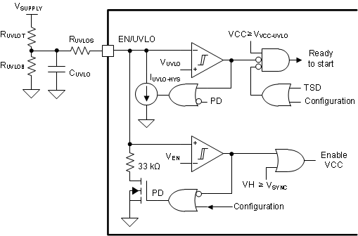
The device shuts down when EN is less than the EN threshold (VEN) and VH is less than the SYNC threshold (VSYNC). The device is enabled when EN is greater than VEN or VH is greater than VSYNC. The VH pin provides a 40-μs internal delay before the device shuts down.
During shutdown, a 33-kΩ internal pulldown resistor on the EN pin is connected to GND to prevent a false turn-on when the pin is floating. Once EN goes above the EN threshold (VEN), the 33-kΩ resistor is disconnected and the IUVLO-HYS current source is enabled to provide the UVLO functionality. The IUVLO-HYS current is designed to avoid chatter around the EN threshold voltage.
 Figure 9-1 EN/UVLO Circuit