ZHCSPX4A February 2022 – April 2022 LM5152-Q1 , LM51521-Q1
PRODUCTION DATA
- 1 特性
- 2 应用
- 3 说明
- 4 Revision History
- 5 说明(续)
- 6 Device Comparison Table
- 7 Pin Configuration and Functions
- 8 Specifications
-
9 Detailed Description
- 9.1 Overview
- 9.2 Functional Block Diagram
- 9.3
Feature Description
- 9.3.1 Device Enable/Disable (EN, VH Pin)
- 9.3.2 High Voltage VCC Regulator (BIAS, VCC Pin)
- 9.3.3 Light Load Switching Mode Selection (MODE Pin)
- 9.3.4 Line Undervoltage Lockout (UVLO Pin)
- 9.3.5 Fast Restart Using VCC HOLD (VH Pin)
- 9.3.6 Adjustable Output Regulation Target (VOUT, TRK, VREF Pin)
- 9.3.7 Overvoltage Protection (VOUT Pin)
- 9.3.8 Boost Status Indicator (STATUS Pin)
- 9.3.9 Dynamically Programmable Switching Frequency (RT)
- 9.3.10 External Clock Synchronization (SYNC Pin)
- 9.3.11 Programmable Spread Spectrum (DITHER Pin)
- 9.3.12 Programmable Soft Start (SS Pin)
- 9.3.13 Wide Bandwidth Transconductance Error Amplifier and PWM (TRK, COMP Pin)
- 9.3.14 Current Sensing and Slope Compensation (CSP, CSN Pin)
- 9.3.15 Constant Peak Current Limit (CSP, CSN Pin)
- 9.3.16 Maximum Duty Cycle and Minimum Controllable On-Time Limits
- 9.3.17 Deep Sleep Mode and Bypass Operation (HO, CP Pin)
- 9.3.18 MOSFET Drivers, Integrated Boot Diode, and Hiccup Mode Fault Protection (LO, HO, HB Pin)
- 9.3.19 Thermal Shutdown Protection
- 9.4 Device Functional Modes
- 10Application and Implementation
- 11Power Supply Recommendations
- 12Layout
- 13Device and Documentation Support
- 14Mechanical, Packaging, and Orderable Information
9.3.14 Current Sensing and Slope Compensation (CSP, CSN Pin)
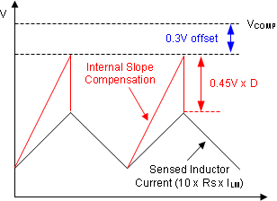
The device features a current sense amplifier with an effective gain of 10 (ACS), and provides an internal slope compensation ramp to the PWM comparator to prevent a subharmonic oscillation at high duty cycle. The device generates the 45-mV peak slope compensation ramp (VSLOPE) at the input of the current sense amplifier, which is a 0.45-V peak (at 100% duty cycle) slope compensation ramp at the PWM comparator input.
According to peak current mode control theory, the slope of the slope compensation ramp must be greater than at least half of the sensed inductor current falling slope to prevent subharmonic oscillation at high duty cycle. Therefore, the minimum amount of the slope compensation must satisfy Equation 10.
where
- 1.5-1.7 is recommended as the margin to cover non-ideal factors.
 Figure 9-15 PWM Comparator Input