ZHCSMC1B october 2020 – august 2023 LM5157-Q1 , LM51571-Q1
PRODUCTION DATA
- 1
- 1 特性
- 2 应用
- 3 说明
- 4 Revision History
- 5 说明(续)
- 6 Device Comparison Table
- 7 Pin Configuration and Functions
- 8 Specifications
-
9 Detailed Description
- 9.1 Overview
- 9.2 Functional Block Diagram
- 9.3
Feature Description
- 9.3.1 Line Undervoltage Lockout (UVLO/SYNC/EN Pin)
- 9.3.2 High Voltage VCC Regulator (BIAS, VCC Pin)
- 9.3.3 Soft Start (SS Pin)
- 9.3.4 Switching Frequency (RT Pin)
- 9.3.5 Dual Random Spread Spectrum – DRSS (MODE Pin)
- 9.3.6 Clock Synchronization (UVLO/SYNC/EN Pin)
- 9.3.7 Current Sense and Slope Compensation
- 9.3.8 Current Limit and Minimum On Time
- 9.3.9 Feedback and Error Amplifier (FB, COMP Pin)
- 9.3.10 Power-Good Indicator (PGOOD Pin)
- 9.3.11 Hiccup Mode Overload Protection (MODE Pin)
- 9.3.12 Maximum Duty Cycle Limit and Minimum Input Supply Voltage
- 9.3.13 Internal MOSFET (SW Pin)
- 9.3.14 Overvoltage Protection (OVP)
- 9.3.15 Thermal Shutdown (TSD)
- 9.4 Device Functional Modes
- 10Application and Implementation
- 11Power Supply Recommendations
- 12Layout
- 13Device and Documentation Support
- 14Mechanical, Packaging, and Orderable Information
9.3.5 Dual Random Spread Spectrum – DRSS (MODE Pin)
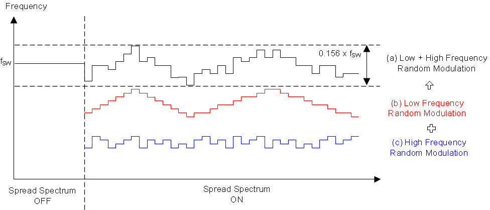
The device provides a digital spread spectrum, which reduces the EMI of the power supply over a wide frequency range. This function is enabled by a single resistor (37.4 kΩ or 100 kΩ) between the MODE pin and the AGND pin or by programming the MODE pin voltage (370 mV or greater than 1.0 V) during initial power up. When the spread spectrum is enabled, the internal modulator dithers the internal clock. When an external synchronization clock is applied to the SYNC pin, the internal spread spectrum is disabled. DRSS (a) combines a low frequency triangular modulation profile (b) with a high frequency cycle-by-cycle random modulation profile (c). The low frequency triangular modulation improves performance in lower radio frequency bands (for example, AM band), while the high frequency random modulation improves performance in higher radio frequency bands (for example, FM band). In addition, the frequency of the triangular modulation is further modulated randomly to reduce the likelihood of any audible tones. In order to minimize output voltage ripple caused by spread spectrum, duty cycle is modified on a cycle-by-cycle basis to maintain a nearly constant duty cycle when dithering is enabled (see Figure 9-9).
 Figure 9-9 Dual Random Spread Spectrum