ZHCSDV5C July   2015  – October 2018 LM5160-Q1

PRODUCTION DATA.  

  1. 特性
  2. 应用
  3. 说明
    1.     Device Images
      1.      典型同步降压应用电路
      2.      典型 Fly-Buck 应用电路
  4. 修订历史记录
  5. Pin Configuration and Functions
    1.     Pin Functions
  6. Specifications
    1. 6.1 Absolute Maximum Ratings
    2. 6.2 ESD Ratings
    3. 6.3 Recommended Operating Conditions
    4. 6.4 Thermal Information
    5. 6.5 Electrical Characteristics
    6. 6.6 Switching Characteristics
    7. 6.7 Typical Characteristics
  7. Detailed Description
    1. 7.1 Overview
    2. 7.2 Functional Block Diagram
    3. 7.3 Feature Description
      1. 7.3.1  Control Circuit
      2. 7.3.2  VCC Regulator
      3. 7.3.3  Regulation Comparator
      4. 7.3.4  Soft Start
      5. 7.3.5  Error Amplifier
      6. 7.3.6  On-Time Generator
      7. 7.3.7  Current Limit
      8. 7.3.8  N-Channel Buck Switch and Driver
      9. 7.3.9  Synchronous Rectifier
      10. 7.3.10 Enable / Undervoltage Lockout (EN/UVLO)
      11. 7.3.11 Thermal Protection
    4. 7.4 Device Functional Modes
      1. 7.4.1 Forced Pulse Width Modulation (FPWM) Mode
      2. 7.4.2 Undervoltage Detector
  8. Application and Implementation
    1. 8.1 Application Information
      1. 8.1.1 Ripple Configuration
    2. 8.2 Typical Applications
      1. 8.2.1 LM5160-Q1 Synchronous Buck (10-V to 60-V Input, 5-V Output, 1.5-A Load)
        1. 8.2.1.1 Design Requirements
        2. 8.2.1.2 Detailed Design Procedure
          1. 8.2.1.2.1  Custom Design With WEBENCH® Tools
          2. 8.2.1.2.2  Feedback Resistor Divider - RFB1, RFB2
          3. 8.2.1.2.3  Switching Frequency - RON
          4. 8.2.1.2.4  Inductor - L
          5. 8.2.1.2.5  Output Capacitor - COUT
          6. 8.2.1.2.6  Series Ripple Resistor - RESR
          7. 8.2.1.2.7  VCC and Bootstrap Capacitors - CVCC, CBST
          8. 8.2.1.2.8  Input Capacitor - CIN
          9. 8.2.1.2.9  Soft-Start Capacitor - CSS
          10. 8.2.1.2.10 EN/UVLO Resistors - RUV1, RUV2
        3. 8.2.1.3 Application Curves
      2. 8.2.2 LM5160-Q1 Isolated Fly-Buck (18-V to 32-V Input, 12-V, 4.5-W Isolated Output)
        1. 8.2.2.1 LM5160-Q1 Fly-Buck Design Requirements
        2. 8.2.2.2 Detailed Design Procedure
          1. 8.2.2.2.1 Selection of VOUT1 and Turns Ratio
          2. 8.2.2.2.2 Secondary Rectifier Diode
          3. 8.2.2.2.3 External Ripple Circuit
          4. 8.2.2.2.4 Output Capacitor - COUT2
        3. 8.2.2.3 Application Curves
    3. 8.3 Do's and Don'ts
  9. Power Supply Recommendations
  10. 10Layout
    1. 10.1 Layout Guidelines
    2. 10.2 Layout Example
  11. 11器件和文档支持
    1. 11.1 器件支持
      1. 11.1.1 第三方米6体育平台手机版_好二三四免责声明
      2. 11.1.2 开发支持
        1. 11.1.2.1 使用 WEBENCH® 工具创建定制设计
    2. 11.2 文档支持
      1. 11.2.1 相关文档
    3. 11.3 接收文档更新通知
    4. 11.4 社区资源
    5. 11.5 商标
    6. 11.6 静电放电警告
    7. 11.7 术语表
  12. 12机械、封装和可订购信息

封装选项

机械数据 (封装 | 引脚)
散热焊盘机械数据 (封装 | 引脚)
订购信息

Typical Characteristics

TA = 25°C, unless otherwise noted. Please refer to Typical Applications for circuit designs.
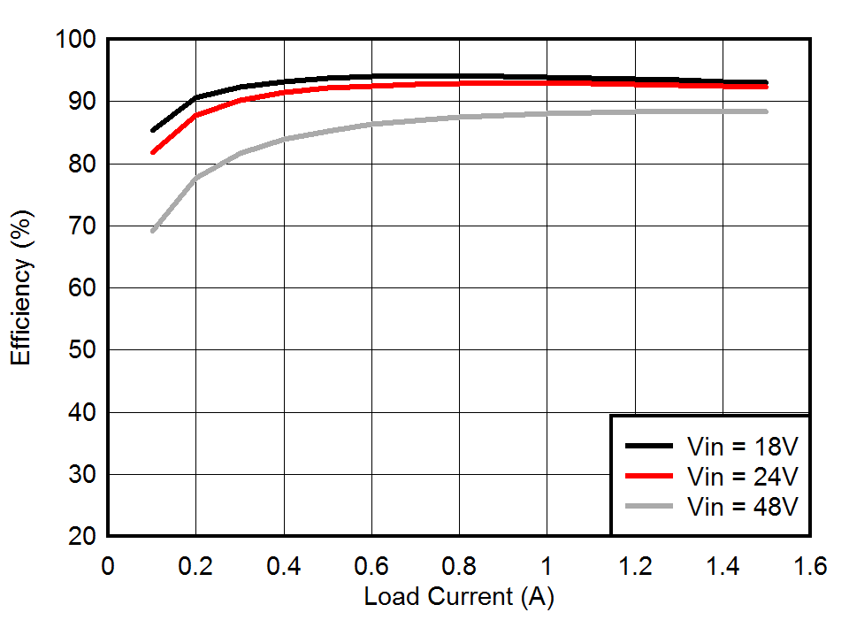
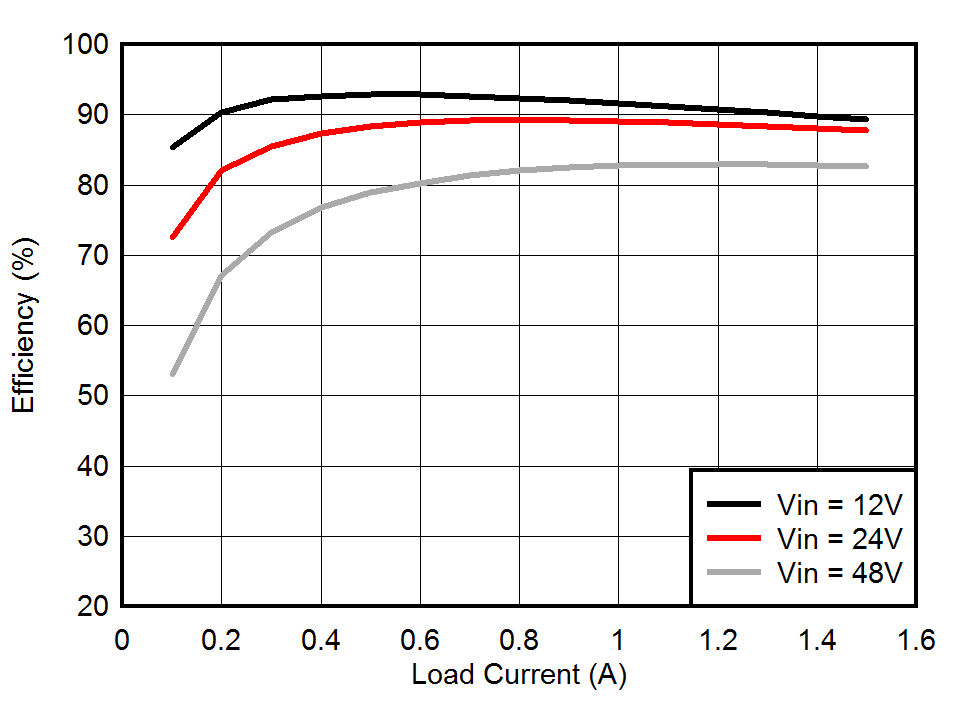
LM5160-Q1 Eff_10Vo_Updated_SNVSA03.gif
VOUT = 10 V RON = 200 kΩ
L = 47 µH
Figure 1. Efficiency at 500 kHz
LM5160-Q1 CCM_DCM_Eff_SNVSA03.gif
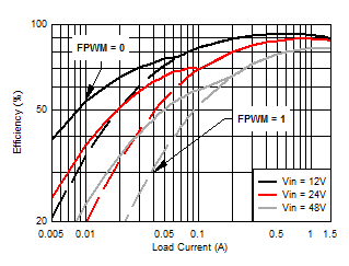
VOUT = 5 V RON = 169 kΩ
L = 47 µH
Figure 3. Efficiency CCM vs DCM at 300 kHz
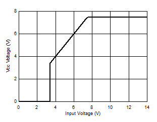
LM5160-Q1 Vcc_Vin_SNVSA03.gif
Figure 5. VCC vs VIN
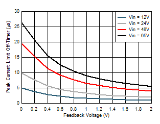
LM5160-Q1 ILim_OffTimer_SNVSA03.gif
Figure 7. TOFF (ILIM) vs VFB
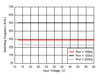
LM5160-Q1 Fsw_Vin_SNVSA03.gif
VOUT = 5 V
Figure 9. Switching Frequency vs VIN
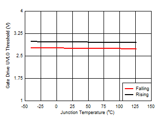
LM5160-Q1 Gate Drive UVLO_Revised_SNVSA03.gif
VIN = 24 V
Figure 11. Gate Drive UVLO vs Temperature
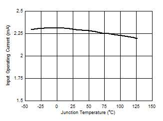
LM5160-Q1 Operating Current_SNVSA03.gif
VIN = 24 V
Figure 13. Input Operating Current vs Temperature
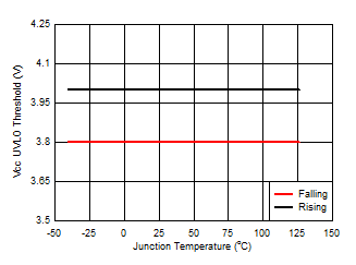
LM5160-Q1 Vcc UVLO Threshold_SNVSA03.gif
VIN = 24 V
Figure 15. VCC UVLO vs Temperature
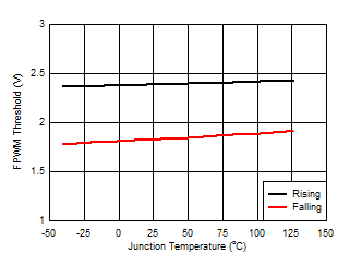
LM5160-Q1 FPWM_Revised_SNVSA03.gif
VIN = 24 V
Figure 17. FPWM Threshold vs Temperature
LM5160-Q1 Eff_250kHz_SNVSA03.gif
VOUT = 5 V RON = 215 kΩ
L = 100 µH
Figure 2. Efficiency at 250 kHz
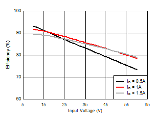
LM5160-Q1 Eff vs Vin Updated_SNVSA03.gif
VOUT = 5 V RON = 169 kΩ
L = 47 µH
Figure 4. Efficiency vs Input Voltage at 300 kHz
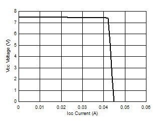
LM5160-Q1 Vcc_Icc_SNVSA03.gif
VIN = 24 V
Figure 6. VCC vs ICC
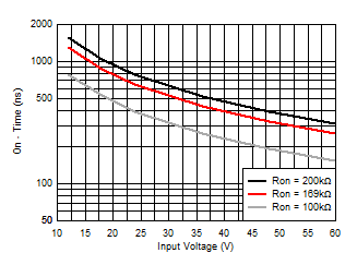
LM5160-Q1 On-Time_Vin_SNVSA03.gif
VOUT = 5 V
Figure 8. TON vs VIN
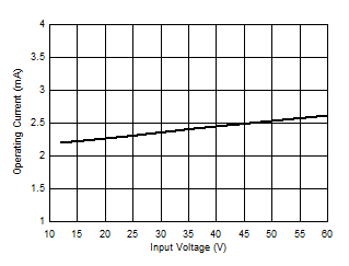
LM5160-Q1 Operating Current vs. Vin _Revised_SNVSA03.gif
VFB = 3 V
Figure 10. IIN vs VIN (Operating, Non-Switching)
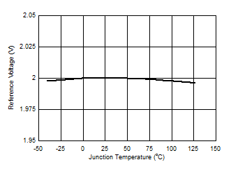
LM5160-Q1 Vref_vs_Temp_LM5160_SNVSA03.gif
VIN = 24 V
Figure 12. Reference Voltage vs Temperature
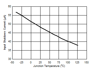
LM5160-Q1 Shutdown_Current_SNVSA03.gif
VIN = 24 V
Figure 14. Input Shutdown Current vs Temperature
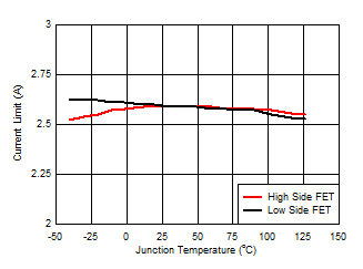
LM5160-Q1 Current Limit_SNVSA03.gif
VIN = 24 V
Figure 16. Current Limit vs Temperature
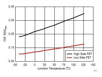
LM5160-Q1 FET_Rdson_SNVSA03.gif
ISW = 200 mA VIN = 24 V
Figure 18. Switch Resistance vs Temperature