ZHCSDV5C July 2015 – October 2018 LM5160-Q1
PRODUCTION DATA.
- 1 特性
- 2 应用
- 3 说明
- 4 修订历史记录
- 5 Pin Configuration and Functions
- 6 Specifications
- 7 Detailed Description
-
8 Application and Implementation
- 8.1 Application Information
- 8.2
Typical Applications
- 8.2.1
LM5160-Q1 Synchronous Buck (10-V to 60-V Input, 5-V Output, 1.5-A Load)
- 8.2.1.1 Design Requirements
- 8.2.1.2
Detailed Design Procedure
- 8.2.1.2.1 Custom Design With WEBENCH® Tools
- 8.2.1.2.2 Feedback Resistor Divider - RFB1, RFB2
- 8.2.1.2.3 Switching Frequency - RON
- 8.2.1.2.4 Inductor - L
- 8.2.1.2.5 Output Capacitor - COUT
- 8.2.1.2.6 Series Ripple Resistor - RESR
- 8.2.1.2.7 VCC and Bootstrap Capacitors - CVCC, CBST
- 8.2.1.2.8 Input Capacitor - CIN
- 8.2.1.2.9 Soft-Start Capacitor - CSS
- 8.2.1.2.10 EN/UVLO Resistors - RUV1, RUV2
- 8.2.1.3 Application Curves
- 8.2.2 LM5160-Q1 Isolated Fly-Buck (18-V to 32-V Input, 12-V, 4.5-W Isolated Output)
- 8.2.1
LM5160-Q1 Synchronous Buck (10-V to 60-V Input, 5-V Output, 1.5-A Load)
- 8.3 Do's and Don'ts
- 9 Power Supply Recommendations
- 10Layout
- 11器件和文档支持
- 12机械、封装和可订购信息
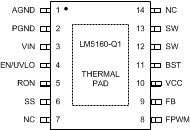
5 Pin Configuration and Functions
Pin Functions
| PIN | I/O(1) | DESCRIPTION | |
|---|---|---|---|
| NO. | NAME | ||
| 1 | AGND | — | Analog Ground. Ground connection of internal control circuits. |
| 2 | PGND | P | Power Ground. Ground connection of the internal synchronous rectifier FET. |
| 3 | VIN | P | Input supply connection. Operating input range is 4.5 V to 65 V. |
| 4 | EN/UVLO | I | Precision enable. Input pin of undervoltage lockout (UVLO) comparator. |
| 5 | RON | I | On-time programming pin. A resistor between this pin and VIN sets the switch on-time as a function of input voltage. |
| 6 | SS | I | Soft-start. Connect a capacitor from SS to AGND to control output rise time and limit overshoot. |
| 8 | FPWM | I | Forced PWM logic input pin. Connect to AGND for discontinuous conduction mode (DCM) with light loads. Connect to VCC for continuous conduction mode (CCM) at all loads and Fly-Buck configuration. |
| 9 | FB | I | Feedback input of voltage regulation comparator. |
| 10 | VCC | O | Internal high voltage start-up regulator bypass capacitor pin. |
| 11 | BST | P | Bootstrap capacitor pin. Connect a capacitor between BST and SW to bias gate driver of high-side buck FET. |
| 12,13 | SW | P | Switch node. Source connection of high-side buck FET and drain connection of low-side synchronous rectifier FET. |
| 7,14 | NC | — | No Connection. |
| — | EP | — | Exposed Pad. Connect to AGND and printed-circuit board ground plane to improve power dissipation. |
(1) P = Power, G = Ground, I = Input, O = Output.
