ZHCSJY6A June 2019 – April 2024 LM5163-Q1
PRODUCTION DATA
- 1
- 1 特性
- 2 应用
- 3 说明
- 4 Pin Configuration and Functions
- 5 Specifications
-
6 Detailed Description
- 6.1 Overview
- 6.2 Functional Block Diagram
- 6.3
Feature Description
- 6.3.1 Control Architecture
- 6.3.2 Internal VCC Regulator and Bootstrap Capacitor
- 6.3.3 Regulation Comparator
- 6.3.4 Internal Soft Start
- 6.3.5 On-Time Generator
- 6.3.6 Current Limit
- 6.3.7 N-Channel Buck Switch and Driver
- 6.3.8 Synchronous Rectifier
- 6.3.9 Enable/Undervoltage Lockout (EN/UVLO)
- 6.3.10 Power Good (PGOOD)
- 6.3.11 Thermal Protection
- 6.4 Device Functional Modes
- 7 Application and Implementation
- 8 Device and Documentation Support
- 9 Revision History
- 10Mechanical, Packaging, and Orderable Information
7.4.1.1 Compact PCB Layout for EMI Reduction
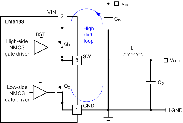
Radiated EMI generated by high di/dt components relates to pulsing currents in switching converters. The larger the area covered by the path of a pulsing current, the more electromagnetic emission is generated. The key to minimizing radiated EMI is to identify the pulsing current path and minimize the area of that path.
Figure 7-16 denotes the critical switching loop of the buck converter power stage in terms of EMI. The topological architecture of a buck converter means that a particularly high di/dt current path exists in the loop comprising the input capacitor and the integrated MOSFETs of the LM5163-Q1, and it becomes mandatory to reduce the parasitic inductance of this loop by minimizing the effective loop area.
 Figure 7-16 DC/DC Buck Converter With Power Stage Circuit Switching Loop
The input capacitor provides the primary path for the high di/dt components of the current of the high-side MOSFET. Placing a ceramic capacitor as close as possible to the VIN and GND pins is the key to EMI reduction. Keep the trace connecting SW to the inductor as short as possible and just wide enough to carry the load current without excessive heating. Use short, thick traces or copper pours (shapes) for current conduction path to minimize parasitic resistance. Place the output capacitor close to the VOUT side of the inductor, and connect the return terminal of the capacitor to the GND pin and exposed PAD of the LM5163-Q1.