ZHCSIT4B September 2018 – April 2024 LM5164-Q1
PRODUCTION DATA
- 1
- 1 特性
- 2 应用
- 3 说明
- 4 Pin Configuration and Functions
- 5 Specifications
-
6 Detailed Description
- 6.1 Overview
- 6.2 Functional Block Diagram
- 6.3
Feature Description
- 6.3.1 Control Architecture
- 6.3.2 Internal VCC Regulator and Bootstrap Capacitor
- 6.3.3 Regulation Comparator
- 6.3.4 Internal Soft Start
- 6.3.5 On-Time Generator
- 6.3.6 Current Limit
- 6.3.7 N-Channel Buck Switch and Driver
- 6.3.8 Synchronous Rectifier
- 6.3.9 Enable/Undervoltage Lockout (EN/UVLO)
- 6.3.10 Power Good (PGOOD)
- 6.3.11 Thermal Protection
- 6.4 Device Functional Modes
- 7 Application and Implementation
- 8 Device and Documentation Support
- 9 Revision History
- 10Mechanical, Packaging, and Orderable Information
4 Pin Configuration and Functions
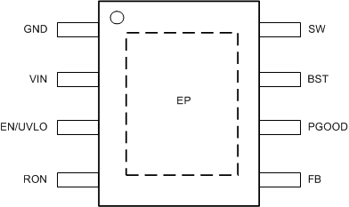
 Figure 4-1 DDA Package8-Pin SO PowerPAD™Top View
Table 4-1 Pin Functions
| PIN | TYPE(1) | DESCRIPTION | |
|---|---|---|---|
| NO. | NAME | ||
| 1 | GND | G | Ground connection for internal circuits |
| 2 | VIN | P/I | Regulator supply input pin to high-side power MOSFET and internal bias regulator. Connect directly to the input supply of the buck converter with short, low impedance paths. |
| 3 | EN/UVLO | I | Precision enable and undervoltage lockout (UVLO) programming pin. If the EN/UVLO voltage is below 1.1 V, the converter is in shutdown mode with all functions disabled. If the UVLO voltage is greater than 1.1 V and below 1.5 V, the converter is in standby mode with the internal VCC regulator operational and no switching. If the EN/UVLO voltage is above 1.5 V, the start-up sequence begins. |
| 4 | RON | I | On-time programming pin. A resistor between this pin and GND sets the buck switch on-time. |
| 5 | FB | I | Feedback input of voltage regulation comparator |
| 6 | PGOOD | O | Power good indicator. This pin is an open-drain output pin. Connect to a source voltage through an external pullup resistor between 10 kΩ to 100 kΩ. |
| 7 | BST | P/I | Bootstrap gate-drive supply. Required to connect a high-quality 2.2-nF 50-V X7R ceramic capacitor between BST and SW to bias the internal high-side gate driver. |
| 8 | SW | P | Switching node that is internally connected to the source of the high-side NMOS buck switch and the drain of the low-side NMOS synchronous rectifier. Connect to the switching node of the power inductor. |
| — | EP | — | Exposed pad of the package. No internal electrical connection. Solder the EP to the GND pin and connect to a large copper plane to reduce thermal resistance. |
(1) G = Ground, I = Input, O = Output, P = Power