ZHCSES0C March 2016 – December 2022 LM5165-Q1
PRODUCTION DATA
- 1 特性
- 2 应用
- 3 说明
- 4 Revision History
- 5 Pin Configuration and Functions
- 6 Specifications
-
7 Detailed Description
- 7.1 Overview
- 7.2 Functional Block Diagram
- 7.3
Feature Description
- 7.3.1 Integrated Power MOSFETs
- 7.3.2 Selectable PFM or COT Mode Converter Operation
- 7.3.3 COT Mode Light-Load Operation
- 7.3.4 Low Dropout Operation and 100% Duty Cycle Mode
- 7.3.5 Adjustable Output Voltage (FB)
- 7.3.6 Adjustable Current Limit
- 7.3.7 Precision Enable (EN) and Hysteresis (HYS)
- 7.3.8 Power Good (PGOOD)
- 7.3.9 Configurable Soft Start (SS)
- 7.3.10 Thermal Shutdown
- 7.4 Device Functional Modes
-
8 Applications and Implementation
- 8.1 Application Information
- 8.2
Typical Applications
- 8.2.1 Design 1: Wide VIN, Low IQ COT Converter Rated at 5 V, 150 mA
- 8.2.2 Design 2: Small Solution Size PFM Converter Rated at 3.3 V, 50 mA
- 8.2.3 Design 3: High Density 12-V, 75-mA PFM Converter
- 8.2.4 Design 4: 3.3-V, 150-mA COT Converter With High Efficiency
- 8.2.5 Design 5: 15-V, 150-mA, 600-kHz COT Converter
- 8.3 Power Supply Recommendations
- 8.4 Layout
- 9 Device and Documentation Support
- 10Mechanical, Packaging, and Orderable Information
封装选项
机械数据 (封装 | 引脚)
散热焊盘机械数据 (封装 | 引脚)
- DRC|10
订购信息
8.4.1.1 Compact PCB Layout for EMI Reduction
Radiated EMI generated by high di/dt components relates to pulsing currents in switching converters. The larger area covered by the path of a pulsing current, the more electromagnetic emission is generated. The key to minimize radiated EMI is to identify the pulsing current path and minimize the area of that path.
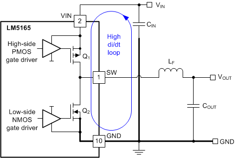
The critical switching loop of the power stage in terms of EMI is denoted in Figure 8-36. The topological architecture of a buck converter means that a particularly high di/dt current effective path exists in the loop comprising the input capacitor and the LM5165-Q1 integrated MOSFETs, and it becomes mandatory to reduce the parasitic inductance of this loop by minimizing the effective loop area.
 Figure 8-36 Synchronous Buck Converter With Power Stage Critical Switching Loop
The input capacitor provides the primary path for the high di/dt components of the high-side MOSFET current. Placing a ceramic capacitor as close as possible to the VIN and GND pins is the key to EMI reduction. Keep the trace connecting SW to the inductor as short as possible and just wide enough to carry the load current without excessive heating. Use short, thick traces or copper pours (shapes) for current conduction path to minimize parasitic resistance. Place the output capacitor close to the VOUT side of the inductor, and connect the capacitor return terminal to the LM5165-Q1 GND pin and exposed PAD.