ZHCSDH1A October 2015 – May 2016 LM5175
PRODUCTION DATA.
- 1 特性
- 2 应用
- 3 说明
- 4 简化电路原理图
- 5 修订历史记录
- 6 Pin Configuration and Functions
- 7 Specifications
-
8 Detailed Description
- 8.1 Overview
- 8.2 Functional Block Diagram
- 8.3
Feature Description
- 8.3.1 Fixed Frequency Valley/Peak Current Mode Control with Slope Compensation
- 8.3.2 VCC Regulator and Optional BIAS Input
- 8.3.3 Enable/UVLO
- 8.3.4 Soft-Start
- 8.3.5 Overcurrent Protection
- 8.3.6 Average Input/Output Current Limiting
- 8.3.7 CCM/DCM Operation
- 8.3.8 Frequency and Synchronization (RT/SYNC)
- 8.3.9 Frequency Dithering
- 8.3.10 Output Overvoltage Protection (OVP)
- 8.3.11 Power Good (PGOOD)
- 8.3.12 Gm Error Amplifier
- 8.3.13 Integrated Gate Drivers
- 8.3.14 Thermal Shutdown
- 8.4 Device Functional Modes
-
9 Application and Implementation
- 9.1 Application Information
- 9.2
Typical Application
- 9.2.1 Design Requirements
- 9.2.2
Detailed Design Procedure
- 9.2.2.1 Frequency
- 9.2.2.2 VOUT
- 9.2.2.3 Inductor Selection
- 9.2.2.4 Output Capacitor
- 9.2.2.5 Input Capacitor
- 9.2.2.6 Sense Resistor (RSENSE)
- 9.2.2.7 Slope Compensation
- 9.2.2.8 UVLO
- 9.2.2.9 Soft-Start Capacitor
- 9.2.2.10 Dither Capacitor
- 9.2.2.11 MOSFETs QH1 and QL1
- 9.2.2.12 MOSFETs QH2 and QL2
- 9.2.2.13 Frequency Compensation
- 9.2.3 Application Curves
- 10Power Supply Recommendations
- 11Layout
- 12器件和文档支持
- 13机械、封装和可订购信息
封装选项
机械数据 (封装 | 引脚)
散热焊盘机械数据 (封装 | 引脚)
订购信息
11 Layout
11.1 Layout Guidelines
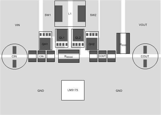
The basic PCB board layout requires separation of sensitive signal and power paths. The following checklist should be followed to get good performance for a well designed board.
- Place the power components including the input filter capacitor CIN, the power MOSFETs QL1 and QH1, and the sense resistor RSENSE close together to minimize the loop area for input switching current in buck operation.
- Place the power components including the output filter capacitor COUT, the power MOSFETs QL2 and QH2, and the sense resistor RSENSE close together to minimize the loop area for output switching current in boost operation.
- Use a combination of bulk capacitors and smaller ceramic capacitors with low series impedance for the input and output capacitors. Place the smaller capacitors closer to the IC to provide a low impedance path for high di/dt switching currents.
- Minimize the SW1 and SW2 loop areas as these are high dv/dt nodes.
- Layout the gate drive traces and return paths as directly as possible. Layout the forward and return traces close together, either running side by side or on top of each other on adjacent layers to minimize the inductance of the gate drive path.
- Use Kelvin connections to RSENSE for the current sense signals CS and CSG and run lines in parallel from the RSENSE terminals to the IC pins. Avoid crossing noisy areas such as SW1 and SW2 nodes or high-side gate drive traces. Place the filter capacitor for the current sense signal as close to the IC pins as possible.
- Place the CIN, COUT, and RSENSE ground pins as close as possible with thick ground trace and/or planes on multiple layers.
- Place the VCC bypass capacitor close to the controller IC, between the VCC and PGND pins. A 1-µF ceramic capacitor is typically used.
- Place the BIAS bypass capacitor close to the controller IC, between the BIAS and PGND pins. A 0.1-µF ceramic capacitor is typically used.
- Place the BOOT1 bootstrap capacitor close to the IC and connect directly to the BOOT1 to SW1 pins.
- Place the BOOT2 bootstrap capacitor close to the IC and connect directly to the BOOT2 to SW2 pins.
- Bypass the VIN pin to AGND with a low ESR ceramic capacitor located close to the controller IC. A 0.1 µF ceramic capacitor is typically used. When using external BIAS, use a diode between input rails and VIN pins to prevent reverse conduction when VIN < VCC.
- Connect the feedback resistor divider between the COUT positive terminal and AGND pin of the IC. Place the components close to the FB pin.
- Use care to separate the power and signal paths so that no power or switching current flows through the AGND connections which can either corrupt the COMP, SLOPE, or SYNC signals, or cause dc offset in the FB sense signal. The PGND and AGND traces can be connected near the PGND pin, near the VCC capacitor PGND connection, or near the PGND connection of the CS, CSG pin current sense resistor.
- When using the average current loop, divide the overall capacitor (CIN or COUT) between the two sides of the sense resistor to ensure small cycle-by-cycle ripple. Place the average current loop filter capacitor close to the IC between the ISNS(+) and ISNS(-) pins.
11.2 Layout Example
 Figure 29. LM5175 Power Stage Layout