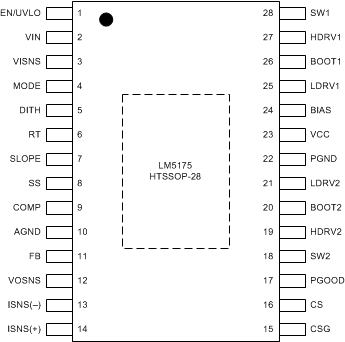
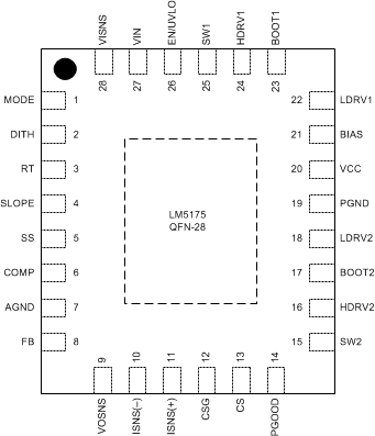
| EN/UVLO |
1 |
26 |
Enable pin. For EN/UVLO < 0.4 V, the LM5175 is in a low current shutdown mode. For 0.7 V < EN/UVLO < 1.23 V, the controller operates in standby mode in which the VCC regulator is enabled but the PWM controller is not switching. For EN/UVLO > 1.23 V, the PWM function is enabled, provided VCC exceeds the VCC UV threshold. |
| VIN |
2 |
27 |
The input supply pin to the IC. Connect VIN to a supply voltage between 3.5 V and 42 V. |
| VISNS |
3 |
28 |
VIN sense input. Connect to the input capacitor. |
| MODE |
4 |
1 |
Mode = GND, DCM, Hiccup Disabled |
(Set RMODE resistor to GND = 0 Ω) |
| Mode = 1.00 V, DCM, Hiccup Enabled |
(Set RMODE resistor to GND = 49.9 kΩ) |
| Mode = 1.85 V, CCM, Hiccup Enabled |
(Set RMODE resistor to GND = 93.1 kΩ) |
| Mode = VCC, CCM, Hiccup Disabled |
(Set RMODE resistor to VCC = 0 Ω) |
| DITH |
5 |
2 |
A capacitor connected between the DITH pin and AGND is charged and discharged with a 10 uA current source. As the voltage on the DITH pin ramps up and down the oscillator frequency is modulated between –5% and +5% of the nominal frequency set by the RT resistor. Grounding the DITH pin will disable the dithering feature. In the external Sync mode, the DITH pin voltage is ignored. |
| RT/SYNC |
6 |
3 |
Switching frequency programming pin. An external resistor is connected to the RT/SYNC pin and AGND to set the switching frequency. This pin can also be used to synchronize the PWM controller to an external clock. |
| SLOPE |
7 |
4 |
A capacitor connected between the SLOPE pin and AGND provides the slope compensation ramp for stable current mode operation in both buck and boost mode. |
| SS |
8 |
5 |
Soft-start programming pin. A capacitor between the SS pin and AGND pin programs soft-start time. |
| COMP |
9 |
6 |
Output of the error amplifier. An external RC network connected between COMP and AGND compensates the regulator feedback loop. |
| AGND |
10 |
7 |
Analog ground of the IC. |
| FB |
11 |
8 |
Feedback pin for output voltage regulation. Connect a resistor divider network from the output of the converter to the FB pin. |
| VOSNS |
12 |
9 |
VOUT sense input. Connect to the output capacitor. |
ISNS(–)
ISNS(+) |
13
14 |
10
11 |
Input or Output Current Sense Amplifier inputs. An optional current sense resistor connected between ISNS(+) and ISNS(–) can be located either on the input side or on the output side of the converter. If the sensed voltage across the ISNS(+) and ISNS(-) pins reaches 50 mV, a slow Constant Current (CC) control loop becomes active and starts discharging the soft-start capacitor to regulated the drop across ISNS(+) and ISNS(-) to 50 mV. Short ISNS(+) and ISNS(-) together to disable this feature. |
| CSG |
15 |
12 |
The negative or ground input to the PWM current sense amplifier. Connect directly to the low-side (ground) of the current sense resistor. |
| CS |
16 |
13 |
The positive input to the PWM current sense amplifier. |
| PGOOD |
17 |
14 |
Power Good open drain output. PGOOD is pulled low when FB is outside a 0.8 V ±10% regulation window. |
SW2
SW1 |
18
28 |
15
25 |
The boost and the buck side switching nodes respectively. |
HDRV2
HDRV1 |
19
27 |
16
24 |
Output of the high-side gate drivers. Connect directly to the gates of the high-side MOSFETs. |
BOOT2
BOOT1 |
20
26 |
17
23 |
An external capacitor is required between the BOOT1, BOOT2 pins and the SW1, SW2 pins respectively to provide bias to the high-side MOSFET gate drivers. |
LDRV2
LDRV1 |
21
25 |
18
22 |
Output of the low-side gate drivers. Connect directly to the gates of the low-side MOSFETs. |
| PGND |
22 |
19 |
Power ground of the IC. The high current ground connection to the low-side gate drivers. |
| VCC |
23 |
20 |
Output of the VCC bias regulator. Connect capacitor to ground. |
| BIAS |
24 |
21 |
Optional input to the VCC bias regulator. Powering VCC from an external supply instead of VIN can reduce power loss at high VIN. For VBIAS > 8 V, the VCC regulator draws power from the BIAS pin. The BIAS pin voltage must not exceed 40 V. |
| PowerPAD™ |
- |
- |
The PowerPAD should be soldered to the analog ground. If possible, use thermal vias to connect to a PCB ground plane for improved power dissipation. |

