ZHCSGN6D June 2017 – August 2021 LM5176
PRODUCTION DATA
- 1 特性
- 2 应用
- 3 说明
- 4 Revision History
- 5 Pin Configuration and Functions
- 6 Specifications
-
7 Detailed Description
- 7.1 Overview
- 7.2 Functional Block Diagram
- 7.3
Feature Description
- 7.3.1 Fixed Frequency Valley/Peak Current Mode Control with Slope Compensation
- 7.3.2 VCC Regulator and Optional BIAS Input
- 7.3.3 Enable/UVLO
- 7.3.4 Soft Start
- 7.3.5 Overcurrent Protection
- 7.3.6 Average Input/Output Current Limiting
- 7.3.7 Operation Above 40-V Input
- 7.3.8 CCM Operation
- 7.3.9 Frequency and Synchronization (RT/SYNC)
- 7.3.10 Frequency Dithering
- 7.3.11 Output Overvoltage Protection (OVP)
- 7.3.12 Power Good (PGOOD)
- 7.3.13 Gm Error Amplifier
- 7.3.14 Integrated Gate Drivers
- 7.3.15 Thermal Shutdown
- 7.4 Device Functional Modes
-
8 Application and Implementation
- 8.1 Application Information
- 8.2
Typical Application
- 8.2.1 Design Requirements
- 8.2.2
Detailed Design Procedure
- 8.2.2.1 Custom Design with WEBENCH Tools
- 8.2.2.2 Frequency
- 8.2.2.3 VOUT
- 8.2.2.4 Inductor Selection
- 8.2.2.5 Output Capacitor
- 8.2.2.6 Input Capacitor
- 8.2.2.7 Sense Resistor (RSENSE)
- 8.2.2.8 Slope Compensation
- 8.2.2.9 UVLO
- 8.2.2.10 Soft-Start Capacitor
- 8.2.2.11 Dither Capacitor
- 8.2.2.12 MOSFETs QH1 and QL1
- 8.2.2.13 MOSFETs QH2 and QL2
- 8.2.2.14 Frequency Compensation
- 8.2.3 Application Curves
- 9 Power Supply Recommendations
- 10Layout
- 11Device and Documentation Support
- 12Mechanical, Packaging, and Orderable Information
封装选项
机械数据 (封装 | 引脚)
散热焊盘机械数据 (封装 | 引脚)
订购信息
5 Pin Configuration and Functions
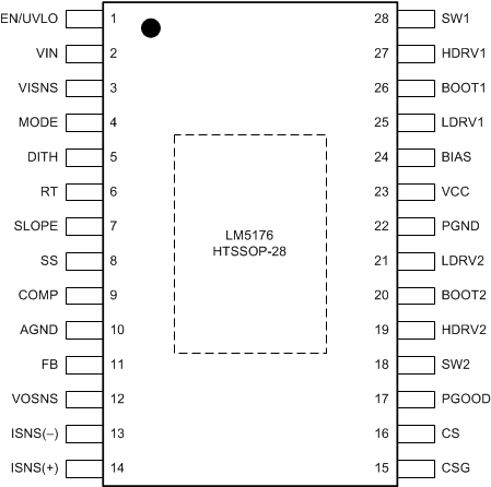
 Figure 5-1 PWP Package28-Pin HTSSOP With PowerPAD™Top View
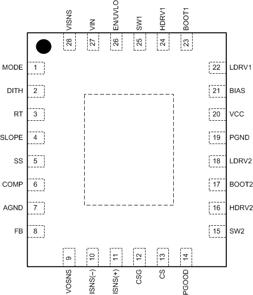
 Figure 5-2 RHF Package
28-Pin QFN With PowerPADTop View
Figure 5-2 RHF Package
28-Pin QFN With PowerPADTop ViewTable 5-1 Pin Functions
| PIN | I/O | DESCRIPTION | ||
|---|---|---|---|---|
| NAME | HTSSOP | QFN | ||
| EN/UVLO | 1 | 26 | I | Enable pin. For EN/UVLO < 0.4 V, the LM5176 is in a low current shutdown mode. For EN/UVLO > 1.22 V, the PWM function is enabled, provided VCC exceeds the VCC UV threshold. |
| VIN | 2 | 27 | I/P | The input supply pin to the IC. Connect VIN to a supply voltage between 4.2 V and 55 V. |
| VISNS | 3 | 28 | I | VIN sense input. Connect to power stage input rail. |
| MODE | 4 | 1 | I | 1.38 V < MODE < 2.22 V: CCM, hiccup enabled (set RMODE resistor to AGND = 93.1 kΩ) |
| 2.6 V < MODE < VCC: CCM, hiccup disabled (set RMODE resistor to AGND = 200 kΩ or connect to VCC) | ||||
| DITH | 5 | 2 | I | A capacitor connected between the DITH pin and AGND is charged and discharged with a current source. As the voltage on the DITH pin ramps up and down the oscillator frequency is modulated by 10% of the nominal frequency set by the RT resistor. Grounding the DITH pin will disable the dithering feature. In the external Sync mode, the DITH pin voltage is ignored. |
| RT/SYNC | 6 | 3 | I | Switching frequency programming pin. An external resistor is connected to the RT/SYNC pin and AGND to set the switching frequency. This pin can also be used to synchronize the PWM controller to an external clock. |
| SLOPE | 7 | 4 | I | A capacitor connected between the SLOPE pin and AGND provides the slope compensation ramp for stable current mode operation in both buck and boost mode. |
| SS | 8 | 5 | I | Soft-start programming pin. A capacitor between the SS pin and AGND pin programs soft-start time. |
| COMP | 9 | 6 | O | Output of the error amplifier. An external RC network connected between COMP and AGND compensates the regulator feedback loop. |
| AGND | 10 | 7 | G | Analog ground of the IC |
| FB | 11 | 8 | I | Feedback pin for output voltage regulation. Connect a resistor divider network from the output of the converter to the FB pin. |
| VOSNS | 12 | 9 | I | VOUT sense input. Connect to the power stage output rail. |
| ISNS(–) ISNS(+) |
13 14 |
10 11 |
I | Input or output current sense amplifier inputs. An optional current sense resistor connected between ISNS(+) and ISNS(–) can be located either on the input side or on the output side of the converter. If the sensed voltage across the ISNS(+) and ISNS(-) pins reaches 50 mV, a slow constant current (CC) control loop becomes active and starts discharging the soft-start capacitor to regulate the drop across ISNS(+) and ISNS(–) to 50 mV. Short ISNS(+) and ISNS(–) together to disable this feature. |
| CSG | 15 | 12 | I | The negative or ground input to the PWM current sense amplifier. Connect directly to the low-side (ground) of the current sense resistor. |
| CS | 16 | 13 | I | The positive input to the PWM current sense amplifier |
| PGOOD | 17 | 14 | O | Power-Good open drain output. PGOOD is pulled low when FB is outside a -9%/+10% regulation window around the 0.8-V VREF. |
| SW2 SW1 |
18 28 |
15 25 |
I | The boost and the buck side switching nodes, respectively. |
| HDRV2 HDRV1 |
19 27 |
16 24 |
O | Output of the high-side gate drivers. Connect directly to the gates of the high-side MOSFETs. |
| BOOT2 BOOT1 |
20 26 |
17 23 |
P | An external capacitor is required between the BOOT1, BOOT2 pins and the SW1, SW2 pins respectively to provide bias to the high-side MOSFET gate drivers. |
| LDRV2 LDRV1 |
21 25 |
18 22 |
O | Output of the low-side gate drivers. Connect directly to the gates of the low-side MOSFETs. |
| PGND | 22 | 19 | G | Power ground of the IC. The high current ground connection to the low-side gate drivers |
| VCC | 23 | 20 | I/O/P | Output of the VCC bias regulator. Connect capacitor to ground. |
| BIAS | 24 | 21 | I/P | Optional input to the VCC bias regulator. Powering VCC from an external supply instead of VIN can reduce power loss at high VIN. For VBIAS > 8 V, the VCC regulator draws power from the BIAS pin. |
| PowerPAD™ | — | — | — | Solder the PowerPAD to the analog ground. If possible, use thermal vias to connect to a PCB ground plane for improved power dissipation. |