ZHCSTC5B October 2023 – June 2024 LM51772
PRODUCTION DATA
- 1
- 1 特性
- 2 应用
- 3 说明
- 4 Pin Configuration and Functions
- 5 Specifications
- 6 Parameter Measurement Information
-
7 Detailed Description
- 7.1 Overview
- 7.2 Functional Block Diagram
- 7.3
Feature Description
- 7.3.1 Buck-Boost Control Scheme
- 7.3.2 Power Save Mode
- 7.3.3 Programmable Conduction Mode PCM
- 7.3.4 Reference System
- 7.3.5 Supply Voltage Selection – VSMART Switch and Selection Logic
- 7.3.6 Enable and Undervoltage Lockout
- 7.3.7 Internal VCC Regulators
- 7.3.8 Error Amplifier and Control
- 7.3.9 Output Voltage Discharge
- 7.3.10 Peak Current Sensor
- 7.3.11 Short Circuit - Hiccup Protection
- 7.3.12 Current Monitor/Limiter
- 7.3.13 Oscillator Frequency Selection
- 7.3.14 Frequency Synchronization
- 7.3.15 Output Voltage Tracking
- 7.3.16 Slope Compensation
- 7.3.17 Configurable Soft Start
- 7.3.18 Drive Pin
- 7.3.19 Dual Random Spread Spectrum – DRSS
- 7.3.20 Gate Driver
- 7.3.21 Cable Drop Compensation (CDC)
- 7.3.22 CFG-pin and R2D Interface
- 7.3.23 Advanced Monitoring Features
- 7.3.24
Protection Features
- 7.3.24.1 Thermal Shutdown (TSD)
- 7.3.24.2 Over Current Protection
- 7.3.24.3 Output Over Voltage Protection 1 (OVP1)
- 7.3.24.4 Output Over Voltage Protection 2 (OVP2)
- 7.3.24.5 Input Voltage Protection (IVP)
- 7.3.24.6 Input Voltage Regulation (IVR)
- 7.3.24.7 Power Good
- 7.3.24.8 Boot-Strap Under Voltage Protection
- 7.3.24.9 Boot-strap Over Voltage Clamp
- 7.3.24.10 CRC - CHECK
- 7.4 Device Functional Modes
- 7.5 Programming
- 8 LM51772 Registers
-
9 Application and Implementation
- 9.1 Application Information
- 9.2
Typical Application
- 9.2.1 Design Requirements
- 9.2.2
Detailed Design Procedure
- 9.2.2.1 Custom Design with WEBENCH Tools
- 9.2.2.2 Frequency
- 9.2.2.3 Feedback Divider
- 9.2.2.4 Inductor and Current Sense Resistor Selection
- 9.2.2.5 Output Capacitor
- 9.2.2.6 Input Capacitor
- 9.2.2.7 Slope Compensation
- 9.2.2.8 UVLO Divider
- 9.2.2.9 Soft-Start Capacitor
- 9.2.2.10 MOSFETs QH1 and QL1
- 9.2.2.11 MOSFETs QH2 and QL2
- 9.2.2.12 Loop Compensation
- 9.2.2.13 External Component Selection
- 9.2.3 Application Curves
- 9.3 Power Supply Recommendations
- 9.4 Layout
- 9.5 USB-PD Source with Power Path
- 9.6 Parallel (Multiphase) Operation
- 9.7 Constant Current LED Driver
- 9.8 Wireless Charging Supply
- 9.9 Bi-Directional Power Backup
- 10Device and Documentation Support
- 11Revision History
- 12Mechanical, Packaging, and Orderable Information
7.3.14 Frequency Synchronization
The device features an internal phase looked loop (PLL), which is designed to transition the switching frequency seamlessly between the frequency set by the RT pin and the external frequency synchronization signal. If no external frequency is provided, the RT pin sets the center frequency of the synchronization range. The external synchronization signal can change the switching frequency ±50%. To ensure low quiescent current, the input buffer of the SYNC pin is disabled if no valid sync frequency, that is a frequency signal outside the recommended synchronization range is applied.
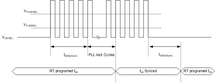
The f(SW) synchronization stops if the device enters power save mode or μSleep operation, if enabled. Once the converter enters the PWM operation again, the device re-syncs to a pin signal. The synchronization timings are given in Figure 7-27
 Figure 7-26 Main Oscillator Functional
Block Diagram
 Figure 7-27 Timing Diagram SYNC
Function
Figure 7-27 Timing Diagram SYNC
FunctionThe SYNC pin can be programmed through I2C or configured via R2D interface:
- As input triggering on the rising edge
- As input triggering on the falling edge (180deg phase shift)
- As an output of the main oscillator clock