ZHCSII9C July   2018  – April 2019 LM5180-Q1

PRODUCTION DATA.  

  1. 特性
  2. 应用
  3. 说明
    1.     Device Images
      1.      典型应用
      2.      典型效率 (VOUT = 5V)
  4. 修订历史记录
  5. Pin Configuration and Functions
    1.     Pin Functions
  6. Specifications
    1. 6.1 Absolute Maximum Ratings
    2. 6.2 ESD Ratings
    3. 6.3 Recommended Operating Conditions
    4. 6.4 Thermal Information
    5. 6.5 Electrical Characteristics
    6. 6.6 Typical Characteristics
  7. Detailed Description
    1. 7.1 Overview
    2. 7.2 Functional Block Diagram
    3. 7.3 Feature Description
      1. 7.3.1  Integrated Power MOSFET
      2. 7.3.2  PSR Flyback Modes of Operation
      3. 7.3.3  Setting the Output Voltage
        1. 7.3.3.1 Diode Thermal Compensation
      4. 7.3.4  Control Loop Error Amplifier
      5. 7.3.5  Precision Enable
      6. 7.3.6  Configurable Soft Start
      7. 7.3.7  External Bias Supply
      8. 7.3.8  Minimum On-Time and Off-Time
      9. 7.3.9  Overcurrent Protection
      10. 7.3.10 Thermal Shutdown
    4. 7.4 Device Functional Modes
      1. 7.4.1 Shutdown Mode
      2. 7.4.2 Standby Mode
      3. 7.4.3 Active Mode
  8. Application and Implementation
    1. 8.1 Application Information
    2. 8.2 Typical Applications
      1. 8.2.1 Design 1: Wide VIN, Low IQ PSR Flyback Converter Rated at 5 V, 1 A
        1. 8.2.1.1 Design Requirements
        2. 8.2.1.2 Detailed Design Procedure
          1. 8.2.1.2.1  Custom Design With WEBENCH® Tools
          2. 8.2.1.2.2  Custom Design With Excel Quickstart Tool
          3. 8.2.1.2.3  Flyback Transformer – T1
          4. 8.2.1.2.4  Flyback Diode – DFLY
          5. 8.2.1.2.5  Zener Clamp Circuit – DF, DCLAMP
          6. 8.2.1.2.6  Output Capacitor – COUT
          7. 8.2.1.2.7  Input Capacitor – CIN
          8. 8.2.1.2.8  Feedback Resistor – RFB
          9. 8.2.1.2.9  Thermal Compensation Resistor – RTC
          10. 8.2.1.2.10 UVLO Resistors – RUV1, RUV2
          11. 8.2.1.2.11 Soft-Start Capacitor – CSS
        3. 8.2.1.3 Application Curves
      2. 8.2.2 Design 2: PSR Flyback Converter With Dual Outputs of 15 V and –7.7 V at 200 mA
        1. 8.2.2.1 Design Requirements
        2. 8.2.2.2 Detailed Design Procedure
          1. 8.2.2.2.1 Flyback Transformer – T1
          2. 8.2.2.2.2 Flyback Diodes – DFLY1 and DFLY2
          3. 8.2.2.2.3 Input Capacitor – CIN
          4. 8.2.2.2.4 Feedback Resistor – RFB
          5. 8.2.2.2.5 UVLO Resistors – RUV1, RUV2
        3. 8.2.2.3 Application Curves
      3. 8.2.3 Design 3: PSR Flyback Converter With Stacked Dual Outputs of 24 V and 5 V
        1. 8.2.3.1 Design Requirements
        2. 8.2.3.2 Detailed Design Procedure
          1. 8.2.3.2.1 Flyback Transformer – T1
          2. 8.2.3.2.2 Feedback Resistor – RFB
          3. 8.2.3.2.3 UVLO Resistors – RUV1, RUV2
        3. 8.2.3.3 Application Curves
  9. Power Supply Recommendations
  10. 10Layout
    1. 10.1 Layout Guidelines
    2. 10.2 Layout Examples
  11. 11器件和文档支持
    1. 11.1 器件支持
      1. 11.1.1 第三方米6体育平台手机版_好二三四免责声明
      2. 11.1.2 开发支持
      3. 11.1.3 使用 WEBENCH® 工具定制设计方案
    2. 11.2 文档支持
      1. 11.2.1 相关文档
    3. 11.3 接收文档更新通知
    4. 11.4 社区资源
    5. 11.5 商标
    6. 11.6 静电放电警告
    7. 11.7 术语表
  12. 12"机械、封装和可订购信息

封装选项

机械数据 (封装 | 引脚)
散热焊盘机械数据 (封装 | 引脚)
订购信息

Application Curves

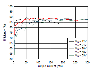
LM5180-Q1 D011_snvsb06.gif
Figure 39. Efficiency (Linear Scale)
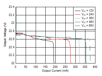
LM5180-Q1 D012_snvsb06.gif
Total of VOUT1 and VOUT2
Figure 41. Load Regulation (Linear Scale)
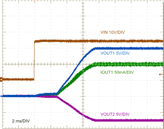
LM5180-Q1 LM5180_design2_startup_waveform_nvsb06.gif
VIN stepped to 24 V 75 Ω and 40 Ω Loads
Figure 43. Start-Up Characteristic
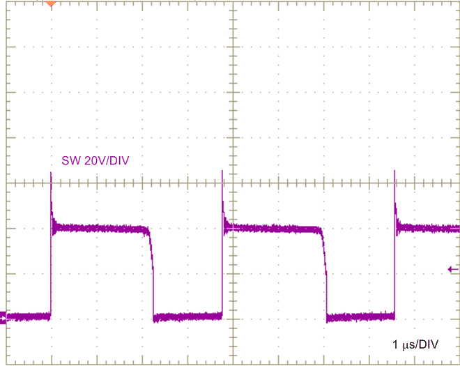
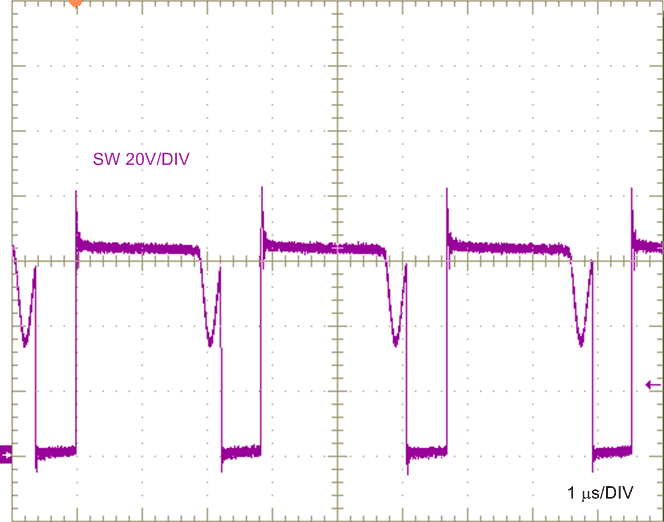
LM5180-Q1 LM5180_design2_SWnode24Vin_waveform_nvsb06.gif
VIN = 24 V
Figure 45. SW Node Voltage, Full Load
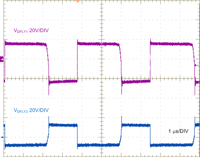
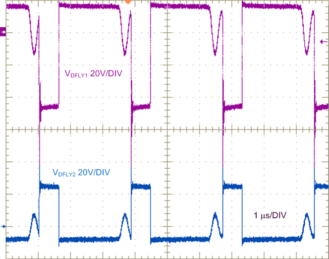
LM5180-Q1 LM5180_design2_24V_VD_waveform_nvsb06.gif
VIN = 24 V
Figure 47. Flyback Diode Voltages, Full Load
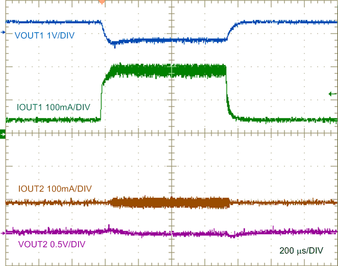
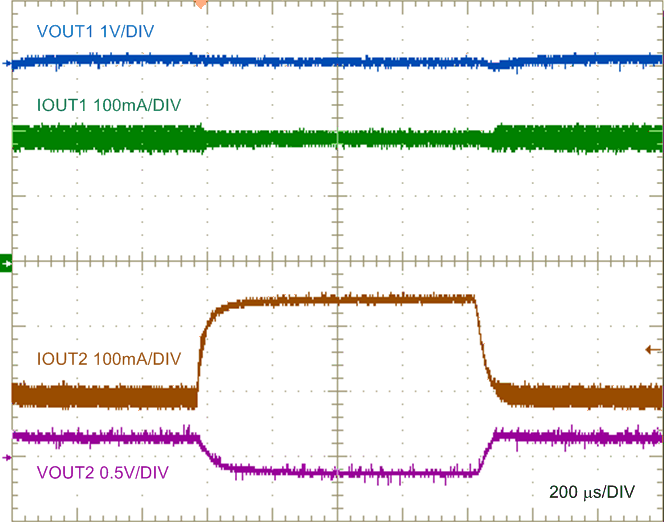
LM5180-Q1 LM5180_design2_load1_transient_waveform_nvsb06.gif
VIN = 24 V IOUT1 = 200 mA
Figure 49. Output 1 Load Transient, 50 mA to 200 mA
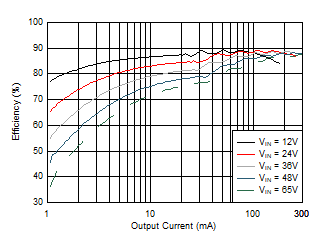
LM5180-Q1 D010_snvsb06.gif
Figure 40. Efficiency (Log Scale)
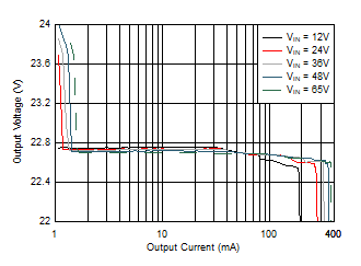
LM5180-Q1 D013_snvsb06.gif
Total of VOUT1 and VOUT2
Figure 42. Load Regulation (Log Scale)
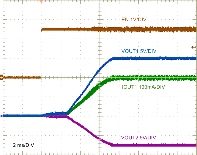
LM5180-Q1 LM5180_design2_ENstartup_waveform_nvsb06.gif
VIN = 24 V 75 Ω and 40 Ω Loads
Figure 44. ENABLE ON Characteristic
LM5180-Q1 LM5180_design2_SWnode48Vin_waveform_nvsb06.gif
VIN = 48 V
Figure 46. SW Node Voltage, Full Load
LM5180-Q1 LM5180_design2_48V_VD_waveform_nvsb06.gif
VIN = 48 V
Figure 48. Flyback Diode Voltages, Full Load
LM5180-Q1 LM5180_design2_load2_transient_waveform_nvsb06.gif
VIN = 24 V IOUT2 = 200 mA
Figure 50. Output 2 Load Transient, 50 mA to 200 mA