ZHCSL48 April 2020 LM5181-Q1
PRODUCTION DATA.
- 1 特性
- 2 应用
- 3 说明
- 4 修订历史记录
- 5 说明 (续)
- 6 Pin Configuration and Functions
- 7 Specifications
-
8 Detailed Description
- 8.1 Overview
- 8.2 Functional Block Diagram
- 8.3
Feature Description
- 8.3.1 Integrated Power MOSFET
- 8.3.2 PSR Flyback Modes of Operation
- 8.3.3 Setting the Output Voltage
- 8.3.4 Control Loop Error Amplifier
- 8.3.5 Precision Enable
- 8.3.6 Configurable Soft Start
- 8.3.7 External Bias Supply
- 8.3.8 Minimum On-Time and Off-Time
- 8.3.9 Overcurrent Protection
- 8.3.10 Thermal Shutdown
- 8.4 Device Functional Modes
-
9 Application and Implementation
- 9.1 Application Information
- 9.2
Typical Applications
- 9.2.1
Design 1: Wide VIN, Low IQ PSR Flyback Converter Rated at 5 V, 0.5 A
- 9.2.1.1 Design Requirements
- 9.2.1.2
Detailed Design Procedure
- 9.2.1.2.1 Custom Design With WEBENCH® Tools
- 9.2.1.2.2 Custom Design With Excel Quickstart Tool
- 9.2.1.2.3 Flyback Transformer – T1
- 9.2.1.2.4 Flyback Diode – DFLY
- 9.2.1.2.5 Zener Clamp Circuit – DF, DCLAMP
- 9.2.1.2.6 Output Capacitor – COUT
- 9.2.1.2.7 Input Capacitor – CIN
- 9.2.1.2.8 Feedback Resistor – RFB
- 9.2.1.2.9 Thermal Compensation Resistor – RTC
- 9.2.1.2.10 UVLO Resistors – RUV1, RUV2
- 9.2.1.2.11 Soft-Start Capacitor – CSS
- 9.2.2 Application Curves
- 9.2.1
Design 1: Wide VIN, Low IQ PSR Flyback Converter Rated at 5 V, 0.5 A
- 10Power Supply Recommendations
- 11Layout
- 12器件和文档支持
- 13机械、封装和可订购信息
8.3.2 PSR Flyback Modes of Operation
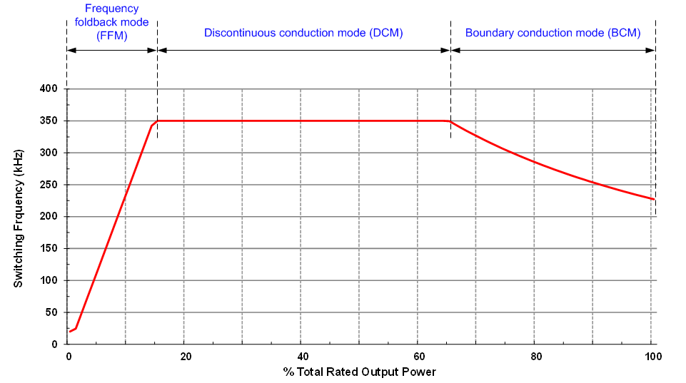
The LM5181-Q1 uses a variable-frequency, peak current-mode (VFPCM) control architecture with three possible modes of operation as illustrated in Figure 18.
 Figure 18. Three Modes of Operation Illustrated by Variation of Switching Frequency With Load
 The LM5181-Q1 operates in boundary conduction mode (BCM) at heavy loads. The power MOSFET turns on when the current in the secondary winding reaches zero, and the MOSFET turns off when the peak primary current reaches the level dictated by the output of the internal error amplifier. As the load is decreased, the frequency increases to maintain BCM operation. The duty cycle of the flyback converter is given Equation 1.

where
- VD is the forward voltage drop of the flyback diode as its current approaches zero
The output power in BCM is given by Equation 2, where the applicable switching frequency and peak primary current in BCM are specified by Equation 3 and Equation 4, respectively.


As the load decreases, the LM5181-Q1 clamps the maximum switching frequency to 350 kHz, and the converter enters discontinuous conduction mode (DCM). The power delivered to the output in DCM is proportional to the peak primary current squared as given by Equation 5 and Equation 6. Thus, as the load decreases, the peak current reduces to maintain regulation at 350-kHz switching frequency.


At even lighter loads, the primary-side peak current set by the internal error amplifier decreases to a minimum level of 0.15 A, or 20% of its 0.75-A peak value, and the MOSFET off-time extends to maintain the output load requirement. The system operates in frequency foldback mode (FFM), and the switching frequency decreases as the load current is reduced. Other than a fault condition, the lowest frequency of operation of the LM5181-Q1 is 12 kHz, which sets a minimum load requirement of approximately 0.5% full load.