ZHCSFV3 November 2016 LM53602 , LM53603
PRODUCTION DATA.
- 1 特性
- 2 应用
- 3 说明
- 4 修订历史记录
- 5 Device Comparison Table
- 6 Pin Configuration and Functions
- 7 Specifications
- 8 Detailed Description
- 9 Application and Implementation
- 10Power Supply Recommendations
- 11Layout
- 12器件和文档支持
- 13机械、封装和可订购信息
8 Detailed Description
8.1 Overview
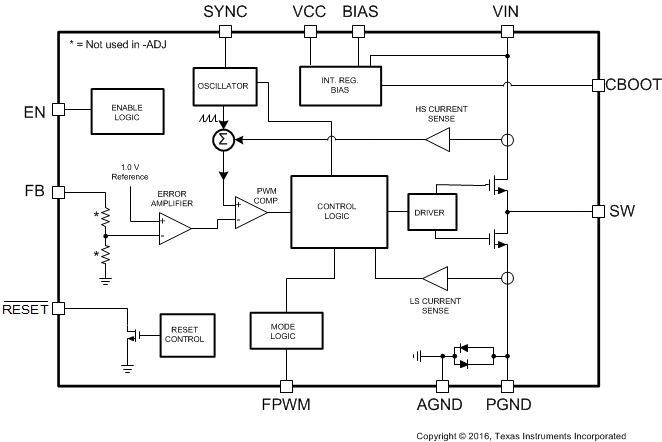
The LM5360x family of devices are synchronous current mode buck regulators designed specifically for the Wide Input voltage Industrial and automotive market. The regulator automatically switches between PWM and PFM depending on load. At heavy loads the device operates in PWM at a switching frequency of 2.1 MHz. The regulator's oscillator can also be synchronized to an external system clock. At input voltages above about 20 V, the switching frequency reduces to maintain regulation during conditions of abnormally high battery voltage. At light loads the mode changes to PFM, with diode emulation allowing DCM. This reduces input supply current and keeps the efficiency high. The user can also choose to lock the mode in PWM (FPWM) so that the switching frequency remains constant regardless of load.
A RESET flag is provided to indicate when the output voltage is near its regulation point. This feature includes filtering and a delay before asserting. This helps to prevent false flag operation during output voltage transients.
Note that, throughout this data sheet, references to the LM53603 apply equally to the LM53602. The difference between the two devices is the maximum output current and specified MOSFET current limits.
8.2 Functional Block Diagram
8.3 Feature Description
8.3.1 RESET Flag Output
The RESET function, built-in to the LM53603, has special features not found in the ordinary Power Good function. A glitch filter prevents false flag operation for short excursions in the output voltage, such as during line and load transients. Furthermore, there is a delay between the point at which the output voltage is within specified limits and the flag asserts Power Good. Because the RESET comparator and the regulation loop share the same reference, the thresholds track with the output voltage. This allows the LM53603 to be specified with a 96.5% maximum threshold, while at the same time specifying a 95% threshold with respect to the actual output voltage for that device. This allows tighter tolerance than is possible with an external supervisor device. The net result is a more accurate power-good function while expanding the system allowance for transients, and so forth. RESET operation can best be understood by reference to Figure 7 and Figure 8. The values for the various filter and delay times can be found in the Timing Requirements table. Output voltage excursions lasting less than TRESET-filter, do not trip RESET. Once the output voltage is within the prescribed limits, a delay of TRESET-act is imposed before RESET goes high.
This output consists of an open-drain NMOS; requiring an external pullup resistor to a suitable logic supply. It can also be pulled up to either VCC or VOUT, through an appropriate resistor, as desired. If this function is not needed, the pin should be left floating or grounded. When EN is pulled low, the flag output is also forced low. With EN low, RESET remains valid as long as the input voltage is ≥ 1.5 V. The maximum current into this pin should be limited to 1 mA, while the maximum voltage should be less than 8 V.
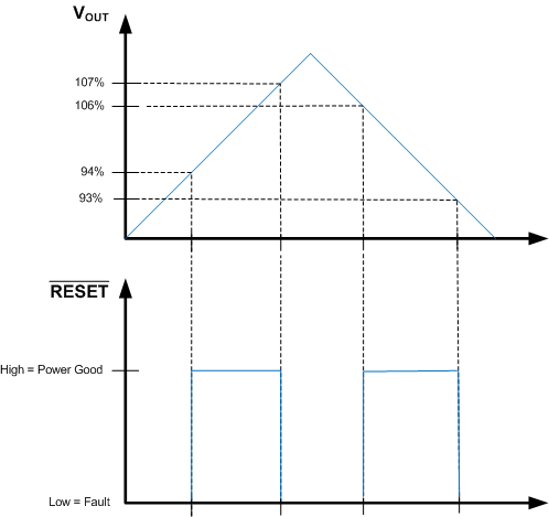 Figure 7. Static RESET Operation
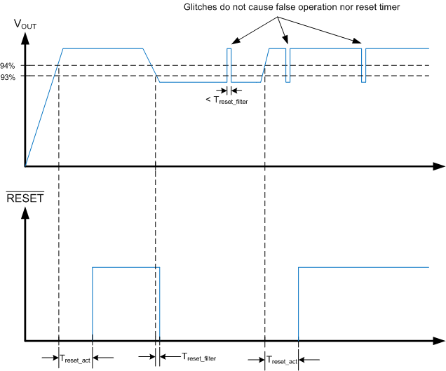 Figure 8. RESET Timing Behavior
8.3.2 Enable and Start-Up
Start-up and shutdown of the LM53603 are controlled by the EN input. Applying a voltage of ≥ 2 V activates the device, while a voltage of ≤ 0.8 V is required to shut it down. The EN input may also be connected directly to the input voltage supply, if this feature is not needed. This input must not be left floating. The LM53603 uses a reference based soft-start, that prevents output voltage overshoots and large inrush currents as the regulator is starting up. A typical start-up waveform is shown in Figure 9 along with typical timings.
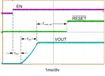 Figure 9. Typical Start-Up Waveform
8.3.3 Current Limit
The LM53603 incorporates valley current limit for normal overloads and for short-circuit protection. In addition, the low side switch is also protected from excessive negative current when the device is in FPWM mode. Finally, a high-side peak current limit is employed for protection of the top NMOS FET.
During overloads the low-side current limit, ILS (see Electrical Characteristics), determines the maximum load current that the LM53603 can supply. When the low-side switch turns on, the inductor current begins to ramp down. If the current does not fall below ILS before the next turnon cycle, then that cycle is skipped and the low-side FET is left on until the current falls below ILS. This is somewhat different than the more typical peak current limit, and results in Equation 1 for the maximum load current.

If the above situation persists for more than about 64 clock cycles, the device turns off both high-side and low-side switches for approximately 5.5 ms (see TW in Timing Requirements). If the overload is still present after the hiccup time, another 64 cycles is counted and the process is repeated. If the current limit is not tripped for two consecutive clock cycles, the counter is reset. Figure 10 shows the inductor current with a hard short on the output. The hiccup time allows the inductor current to fall to zero, resetting the inductor volt-second balance. This is the method used for short-circuit protection and keeps the power dissipation low during a fault. Of course the output current is greatly reduced in this condition (see Typical Characteristics). A typical short-circuit transient and recovery is shown in Figure 11.
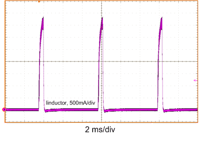 Figure 10. Inductor Current Bursts in Short Circuit
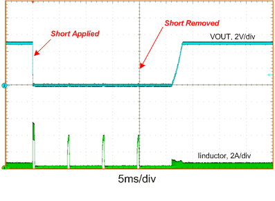 Figure 11. Short-Circuit Transient and Recovery
The high-side current limit trips when the peak inductor current reaches IHS (see Electrical Characteristics). This is a cycle-by-cycle current limit and does not produce any frequency or current fold-back. It is meant to protect the high-side MOSFET from excessive current. Under some conditions, such as high input voltage, this current limit may trip before the low-side protection. The peak value of this current limit varies with duty-cycle.
In FPWM mode, the inductor current is allowed to go negative. Should this current exceed INEG, the low-side switch is turned off until the next clock cycle. This is used to protect the low-side switch from excessive negative current. When the device is in AUTO mode, the negative current limit is increased to about 0 A; IZC. This allows the device to operate in DCM.
8.3.4 Synchronizing Input
The internal clock of the LM53603 can be synchronized to a system clock through the SYNC input. This input recognizes a valid high level as that ≥ 1.5 V, and a valid low as that ≤ 0.4 V. The frequency synchronization signal should be in the range of 1.9 MHz to 2.3 MHz with a duty cycle of from 10% to 90%. The internal clock is synced to the rising edge of the external clock. If this input is not used, it should be grounded. The maximum voltage on this input is 5.5 V; and should not be allowed to float. See the Device Functional Modes section to determine which modes are valid for synchronizing the clock.
8.3.5 Input Supply Current
The LM53603 is designed to have very low input supply current when regulating light loads. One way this is achieved is by powering much of the internal circuitry from the output. The BIAS pin is the input to the LDO that powers the majority of the control circuits. By connecting the BIAS input to the output of the regulator, this current acts as a small load on the output. This current is reduced by the ratio of VOUT/VIN, just like any other load. Another advantage of the LM53603 is that the feedback divider is integrated into the device. This allows the use of much larger resistors than can be used externally; >> 100 kΩ. This results in much lower divider current than is possible with external resistors. Equation 2 can be used to estimate the total input supply current when the device is regulating with no external loads. The terms of the equation are as follows:
- IIN: Input supply current with no load.
- IQ: Device quiescent current, see Electrical Characteristics.
- IEN: Current into EN pin; see Electrical Characteristics.
- IB: Current into BIAS pin; see Electrical Characteristics.
- K: ≈ 0.9

Equation 2 can be used as a guide to indicate how the various terms affect the input supply current. The Application Curves show measured values for the input supply current for both 3.3-V and 5-V output voltage versions.
8.3.6 UVLO and TSD
The LM53603 incorporates an input undervoltage lockout (UVLO) function. The device accepts an EN command when the input voltage rises above about 3.64 V and shuts down when the input falls below about 3.3 V. See the Electrical Characteristics table under VIN-operate for detailed specifications.
Thermal shutdown is provided to protect the device from excessive temperature. When the junction temperature reaches about 162°C, the device shuts down; restart occurs at a temperature of about 144ºC.
8.4 Device Functional Modes
See Table 1 and the following paragraphs for a detailed description of the functional modes for the LM53603. These modes are controlled by the FPWM input as shown in Table 1. This input can be controlled by any compatible logic, and the mode changed while the regulator is operating. If it is desired to lock the mode for a given application, the input can be either connected to ground, a logic supply, or the VCC pin, as desired. The maximum input voltage on this pin is 5.5 V and it should not be allowed to float.
Table 1. Mode Selection
| FPWM INPUT VOLTAGE | OPERATING MODE |
|---|---|
| > 1.5 V | Forced PWM: The regulator operates as a constant frequency, current mode, full-synchronous converter for all loads; without diode emulation. |
| < 0.4 V | AUTO: The regulator moves between PFM and PWM as the load current changes, using diode-emulation-mode to allow DCM (see the Glossary). |
8.4.1 AUTO Mode
In AUTO mode the device moves between PWM and PFM as the load changes. At light loads the regulator operates in PFM. At higher loads the mode changes to PWM. The load currents for which the devices moves from PWM to PFM can be found in the Application Curves.
In PWM , the converter operates as a constant frequency, current mode, full synchronous converter using PWM to regulate the output voltage. While operating in this mode the output voltage is regulated by switching at a constant frequency and modulating the duty cycle to control the power to the load. This provides excellent line and load regulation and low output voltage ripple. When in PWM, the converter synchronizes to any valid clock signal on the SYNC input (see Dropout and Input Voltage Frequency Fold-Back).
In PFM the high-side FET is turned on in a burst of one or more cycles to provide energy to the load. The frequency of these bursts is adjusted to regulate the output, while diode emulation is used to maximize efficiency. This mode provides high light load efficiency by reducing the amount of input supply current required to regulate the output voltage at small loads Glossary. This trades off very good light load efficiency for larger output voltage ripple and variable switching frequency. Also, a small increase in the output voltage occurs in PFM. The actual switching frequency and output voltage ripple depend on the input voltage, output voltage, and load. Typical switching waveforms for PFM are shown in Figure 12. See the Application Curves for output voltage variation in AUTO mode. The SYNC input is ignored during PFM operation.
A unique feature of this device, is that a minimum input voltage is required for the regulator to switch from PWM to PFM at light load. This feature is a consequence of the advanced architecture employed to provide high efficiency at light loads. Figure 13 indicates typical values of input voltage required to switch modes at no-load. Also, once the regulator switches to PFM, at light load, it remains in that mode if the input voltage is reduced.
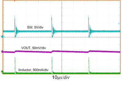 Figure 12. Typical PFM Switching Waveforms
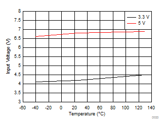 Figure 13. Input Voltage for Mode Change
8.4.2 FPWM Mode
With a logic high on the FPWM input, the device is locked in PWM mode. This operation is maintained, even at no-load, by allowing the inductor current to reverse its normal direction. This mode trades off reduced light load efficiency for low output voltage ripple, tight output voltage regulation, and constant switching frequency. In this mode, a negative current limit of INEG is imposed to prevent damage to the regulators low-side FET. When in FPWM, the converter synchronizes to any valid clock signal on the SYNC input (see Dropout and Input Voltage Frequency Fold-Back).
8.4.3 Dropout
One of the parameters that influences the dropout performance of a buck regulator is the minimum off-time. As the input voltage is reduced, to near the output voltage, the off-time of the high-side switch starts to approach the minimum value (see Timing Requirements). Beyond this point the switching may become erratic or the output voltage falls out of regulation. To avoid this problem, the LM53603 automatically reduces the switching frequency to increase the effective duty cycle. This results in two specifications regarding dropout voltage, as shown in the System Characteristics table. One specification indicates when the switching frequency drops to 1.85 MHz; avoiding the A.M. radio band. The other specification indicates when the output voltage has fallen to 1% of nominal. See the Application Curves for typical values of dropout. The overall dropout characteristic for the 5-V option, can be seen in Figure 14. The SYNC input is ignored during frequency fold-back in dropout.
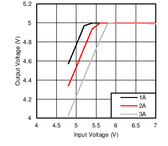 Figure 14. Overall Dropout Characteristic
VOUT = 5V
8.4.4 Input Voltage Frequency Fold-Back
At higher input voltages the on-time of the high-side switch becomes small. When the minimum is reached (see Timing Requirements), the switching may become erratic or the output voltage falls out of regulation. To avoid this behavior, the LM53603 automatically reduces the switching frequency at input voltages above about 20 V (see Application Curves). In this way the device avoids the minimum on-time restriction and maintains regulation at abnormally high battery voltages. The SYNC input is ignored during frequency fold-back at high input voltages.