ZHCSHU8F October 2008 – July 2019 LM5575-Q1
PRODUCTION DATA.
- 1 特性
- 2 应用
- 3 说明
- 4 修订历史记录
- 5 Pin Configuration and Functions
- 6 Specifications
- 7 Detailed Description
- 8 Application and Implementation
- 9 Power Supply Recommendations
- 10Layout
- 11器件和文档支持
- 12机械、封装和可订购信息
7.4.4 Ramp Generator
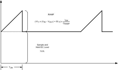
The ramp signal used in the pulse-width modulator for current-mode control is typically derived directly from the buck switch current. This switch current corresponds to the positive slope portion of the output inductor current. Using this signal for the PWM ramp simplifies the control-loop-transfer function to a single pole response and provides inherent input voltage feed-forward compensation. The disadvantage of using the buck switch current signal for PWM control is the large leading edge spike due to circuit parasitics that must be filtered or blanked. Also, the current measurement may introduce significant propagation delays. The filtering, blanking time, and propagation delay limit the minimum achievable pulse width. In applications where the input voltage may be relatively large in comparison to the output voltage, controlling small pulse widths and duty cycles is necessary for regulation. The LM5575-Q1 uses a unique ramp generator, which does not actually measure the buck switch current but rather reconstructs the signal. Reconstructing or emulating the inductor current provides a ramp signal to the PWM comparator that is free of leading edge spikes and measurement or filtering delays. The current reconstruction is comprised of two elements; a sample and hold DC level and an emulated current ramp.
 Figure 12. Composition of Current Sense Signal
 The sample and hold DC level shown in Figure 12 is derived from a measurement of the re-circulating Schottky diode anode current. The re-circulating diode anode should be connected to the IS pin. The diode current flows through an internal current sense resistor between the IS and PGND pins. The voltage level across the sense resistor is sampled and held just prior to the onset of the next conduction interval of the buck switch. The diode current sensing and sample and hold provide the DC level of the reconstructed current signal. The positive slope inductor current ramp is emulated by an external capacitor connected from the RAMP pin to AGND and an internal voltage controlled current source. The ramp current source that emulates the inductor current is a function of the VIN and VOUT voltages per Equation 2:
Proper selection of the RAMP capacitor depends upon the selected value of the output inductor. The value of CRAMP can be selected from Equation 3:
where
- L is the value of the output inductor in Henrys
With this value, the scale factor of the emulated current ramp is approximately equal to the scale factor of the DC level sample and hold (1 V/A). Locate the CRAMP capacitor very close to the device and connect directly to the pins of the IC (RAMP and AGND).
For duty cycles greater than 50%, peak-current-mode control circuits are subject to sub-harmonic oscillation. Sub-harmonic oscillation is normally characterized by observing alternating wide and narrow pulses at the switch node. Add a fixed slope voltage ramp (slope compensation) to the current sense signal to prevent this oscillation. The 50 µA of offset current provided from the emulated current source adds some fixed slope to the ramp signal. In some high-output voltage, high duty cycle applications, additional slope may be required. In these applications, a pullup resistor may be added between the VCC and RAMP pins to increase the ramp slope compensation.
For VOUT > 7.5 V:
Calculate optimal slope current, IOS = VOUT × 10 µA/V.
For example, at VOUT = 10 V, IOS = 100 µA.
Install a resistor from the RAMP pin to VCC:
 Figure 13. RRAMP to VCC for VOUT > 7.5 V