ZHCSKV5 February   2020 LM60430-Q1 , LM60440-Q1

ADVANCE INFORMATION for pre-production products; subject to change without notice.  

  1. 特性
  2. 应用
  3. 说明
    1.     Device Images
      1.      简化原理图
      2.      效率与输出电流间的关系 VOUT = 5V,400kHz
  4. 修订历史记录
  5. Device Comparison Table
  6. Pin Configuration and Functions
    1.     Pin Functions
  7. Specifications
    1. 7.1 Absolute Maximum Ratings
    2. 7.2 ESD Ratings
    3. 7.3 Recommended Operating Conditions
    4. 7.4 Thermal Information
    5. 7.5 Electrical Characteristics
    6. 7.6 Timing Characteristics
    7. 7.7 System Characteristics
  8. Detailed Description
    1. 8.1 Overview
    2. 8.2 Functional Block Diagram
    3. 8.3 Feature Description
      1. 8.3.1 Power-Good Flag Output
      2. 8.3.2 Enable and Start-up
      3. 8.3.3 Current Limit and Short Circuit
      4. 8.3.4 Undervoltage Lockout and Thermal Shutdown
    4. 8.4 Device Functional Modes
      1. 8.4.1 Auto Mode
      2. 8.4.2 Dropout
      3. 8.4.3 Minimum Switch On-Time
  9. Application and Implementation
    1. 9.1 Application Information
    2. 9.2 Typical Application
      1. 9.2.1 Design Requirements
      2. 9.2.2 Detailed Design Procedure
        1. 9.2.2.1  Choosing the Switching Frequency
        2. 9.2.2.2  Setting the Output Voltage
        3. 9.2.2.3  Inductor Selection
        4. 9.2.2.4  Output Capacitor Selection
        5. 9.2.2.5  Input Capacitor Selection
        6. 9.2.2.6  CBOOT
        7. 9.2.2.7  VCC
        8. 9.2.2.8  CFF Selection
        9. 9.2.2.9  External UVLO
        10. 9.2.2.10 Maximum Ambient Temperature
      3. 9.2.3 Application Curves
    3. 9.3 EMI
    4. 9.4 What to Do and What Not to Do
  10. 10Power Supply Recommendations
  11. 11Layout
    1. 11.1 Layout Guidelines
      1. 11.1.1 Ground and Thermal Considerations
    2. 11.2 Layout Example
  12. 12器件和文档支持
    1. 12.1 器件支持
      1. 12.1.1 开发支持
        1. 12.1.1.1 使用 WEBENCH® 工具创建定制设计方案
    2. 12.2 文档支持
      1. 12.2.1 相关文档
    3. 12.3 接收文档更新通知
    4. 12.4 支持资源
    5. 12.5 商标
    6. 12.6 静电放电警告
    7. 12.7 Glossary
  13. 13机械、封装和可订购信息

封装选项

机械数据 (封装 | 引脚)
散热焊盘机械数据 (封装 | 引脚)
订购信息

EMI

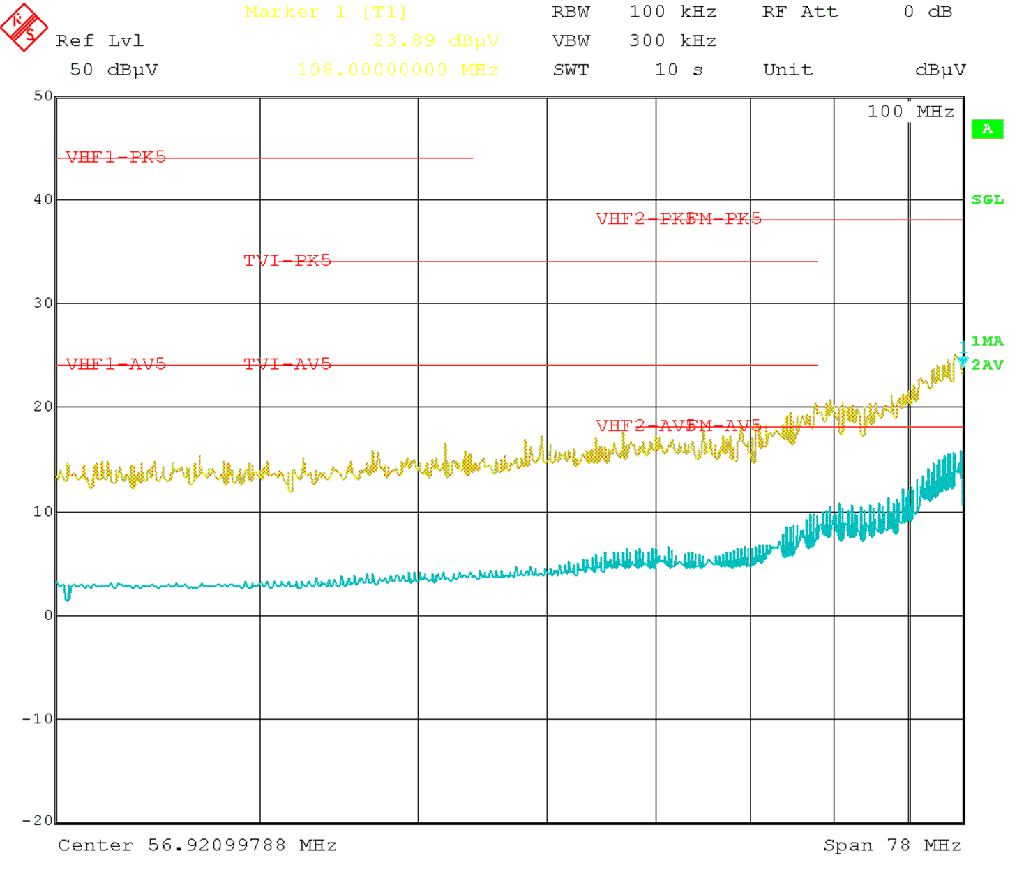
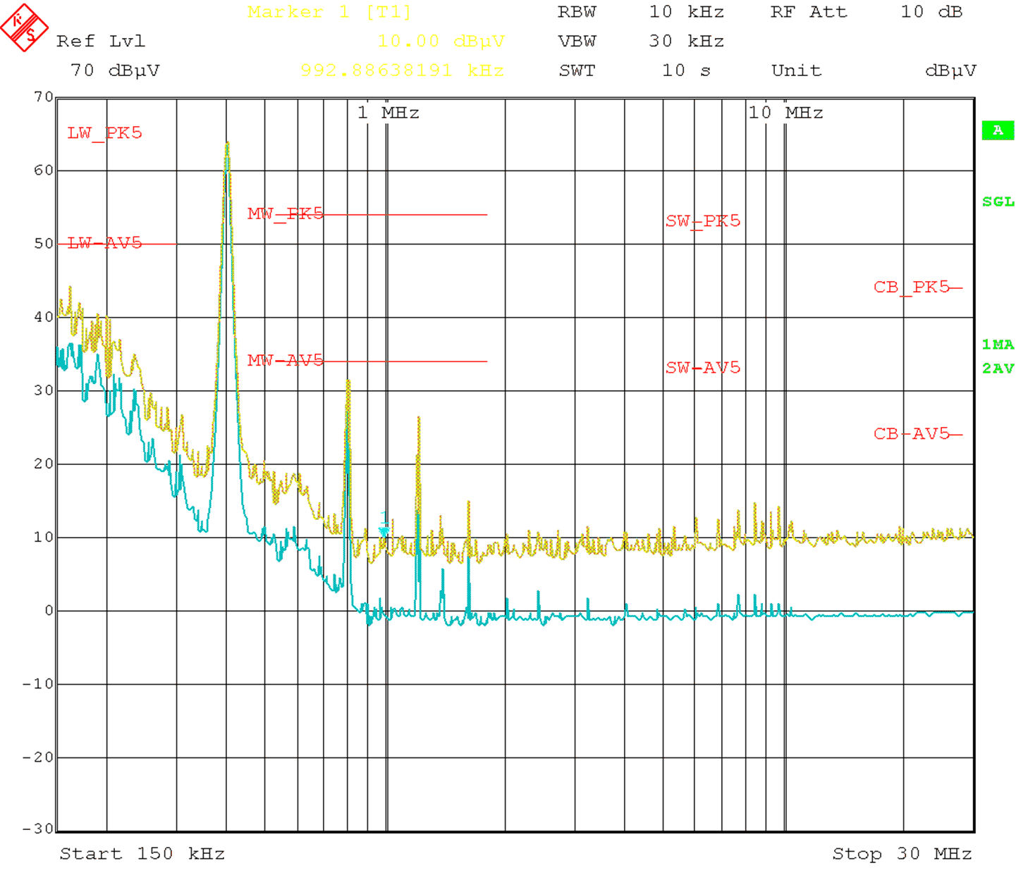
EMI results depend critically on PCB layout and test setup. The results presented here are typical and given for information purposes only. The EMI filter used is shown in Figure 20. The limit lines shown refer to CISPR25 class 5.
LM60440-Q1 LM60430-Q1 EMI_LF_13-5Vin_4A_PR.gif
VIN = 13.5 V VOUT = 5 V IOUT = 4 A
ƒSW = 400 kHz WQFN package
Figure 18. Low Frequency Conducted EMI
LM60440-Q1 LM60430-Q1 EMI_HF_13-5Vin_4A_PR.gif
VIN = 12 V VOUT = 5 V IOUT = A
ƒSW = 400 kHz WQFN package
Figure 19. High Frequency Conducted EMI
LM60440-Q1 LM60430-Q1 EMI-filter-sch-PR.gifFigure 20. Typical Input EMI Filter
Filter Used Only for EMI Measurements Found in EMI