ZHCSKV4 February 2020 LM60430 , LM60440
ADVANCE INFORMATION for pre-production products; subject to change without notice.
- 1 特性
- 2 应用
- 3 说明
- 4 修订历史记录
- 5 Device Comparison Table
- 6 Pin Configuration and Functions
- 7 Specifications
- 8 Detailed Description
- 9 Application and Implementation
- 10Power Supply Recommendations
- 11Layout
- 12器件和文档支持
- 13机械、封装和可订购信息
8.3.1 Power-Good Flag Output
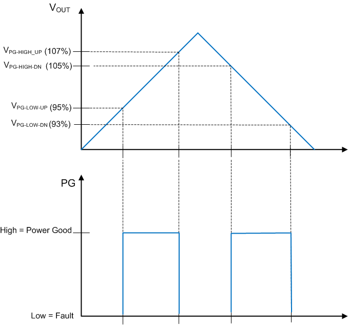
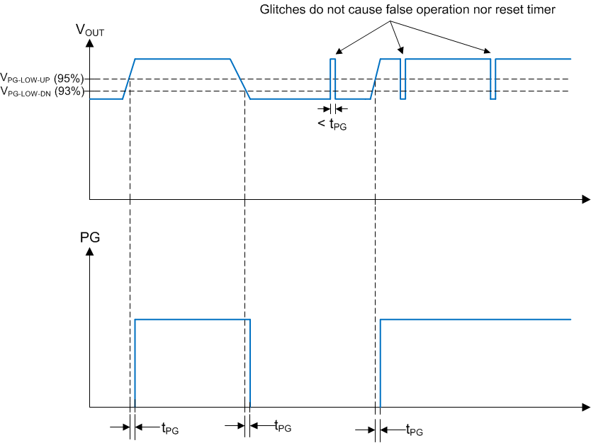
The power-good flag function (PG output pin) of the LM604x0 can be used to reset a system microprocessor whenever the output voltage is out of regulation. This open-drain output goes low under fault conditions, such as current limit and thermal shutdown, as well as during normal start-up. A glitch filter prevents false flag operation for short excursions of the output voltage, such as during line and load transients. The timing parameters of the glitch filter are found in the Electrical Characteristics table. Output voltage excursions lasting less than tPG do not trip the power-good flag. Power-good operation can best be understood by reference to Figure 1 and Figure 2. Note that during initial power up, a delay of about 4 ms (typical) is inserted from the time that EN is asserted to the time that the power-good flag goes high. This delay only occurs during start-up and is not encountered during normal operation of the power-good function.
The power-good output consists of an open-drain NMOS, requiring an external pullup resistor to a suitable logic supply. It can also be pulled up to either VCC or VOUT, through a 100-kΩ resistor, as desired. If this function is not needed, the PG pin must be left floating. When EN is pulled low, the flag output is also forced low. With EN low, power good remains valid as long as the input voltage is ≥ 2 V (typical). Limit the current into the power-good flag pin to less than 5 mA D.C. The maximum current is internally limited to about 35 mA when the device is enabled and about 65 mA when the device is disabled. The internal current limit protects the device from any transient currents that can occur when discharging a filter capacitor connected to this output.
 Figure 1. Static Power-Good Operation
  Figure 2. Power-Good-Timing Behavior