ZHCSMJ1 October 2021 LM61430-Q1
PRODUCTION DATA
- 1 特性
- 2 应用
- 3 说明
- 4 Revision History
- 5 Device Comparison Table
- 6 Pin Configuration and Functions
- 7 Specifications
-
8 Detailed Description
- 8.1 Overview
- 8.2 Functional Block Diagram
- 8.3
Feature Description
- 8.3.1 EN/SYNC Uses for Enable and VIN UVLO
- 8.3.2 EN/SYNC Pin Uses for Synchronization
- 8.3.3 Clock Locking
- 8.3.4 Adjustable Switching Frequency
- 8.3.5 PGOOD Output Operation
- 8.3.6 Internal LDO, VCC UVLO, and BIAS Input
- 8.3.7 Bootstrap Voltage and VCBOOT-UVLO (CBOOT Pin)
- 8.3.8 Adjustable SW Node Slew Rate
- 8.3.9 Spread Spectrum
- 8.3.10 Soft Start and Recovery From Dropout
- 8.3.11 Output Voltage Setting
- 8.3.12 Overcurrent and Short Circuit Protection
- 8.3.13 Thermal Shutdown
- 8.3.14 Input Supply Current
- 8.4 Device Functional Modes
- 9 Application and Implementation
- 10Power Supply Recommendations
- 11Layout
- 12Device and Documentation Support
- 13Mechanical, Packaging, and Orderable Information
8.4.3.2.1 CCM Mode
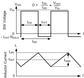
In continuous conduction mode (CCM), the LM61430-Q1 supplies a regulated output voltage by turning on the internal high-side (HS) and low-side (LS) NMOS switches with varying duty cycle (D). During the HS switch on-time, the SW pin voltage, VSW, swings up to approximately VIN, and the inductor current, iL, increases with a linear slope. The HS switch is turned off by the control logic as shown in Section 8.2. During the HS switch off time, tOFF, the LS switch is turned on. Inductor current discharges through the LS switch, which forces the VSW to swing below ground by the voltage drop across the LS switch. Refer to the waveforms in Figure 8-17. The converter loop adjusts the duty cycle to maintain a constant output voltage. D is defined by the on time of the HS switch over the switching period:
In an ideal buck converter where losses are ignored, D is proportional to the output voltage and inversely proportional to the input voltage:
 Figure 8-17 SW Voltage and Inductor Current Waveforms in Continuous Conduction Mode (CCM)