ZHCSMJ1 October 2021 LM61430-Q1
PRODUCTION DATA
- 1 特性
- 2 应用
- 3 说明
- 4 Revision History
- 5 Device Comparison Table
- 6 Pin Configuration and Functions
- 7 Specifications
-
8 Detailed Description
- 8.1 Overview
- 8.2 Functional Block Diagram
- 8.3
Feature Description
- 8.3.1 EN/SYNC Uses for Enable and VIN UVLO
- 8.3.2 EN/SYNC Pin Uses for Synchronization
- 8.3.3 Clock Locking
- 8.3.4 Adjustable Switching Frequency
- 8.3.5 PGOOD Output Operation
- 8.3.6 Internal LDO, VCC UVLO, and BIAS Input
- 8.3.7 Bootstrap Voltage and VCBOOT-UVLO (CBOOT Pin)
- 8.3.8 Adjustable SW Node Slew Rate
- 8.3.9 Spread Spectrum
- 8.3.10 Soft Start and Recovery From Dropout
- 8.3.11 Output Voltage Setting
- 8.3.12 Overcurrent and Short Circuit Protection
- 8.3.13 Thermal Shutdown
- 8.3.14 Input Supply Current
- 8.4 Device Functional Modes
- 9 Application and Implementation
- 10Power Supply Recommendations
- 11Layout
- 12Device and Documentation Support
- 13Mechanical, Packaging, and Orderable Information
8.3.5 PGOOD Output Operation
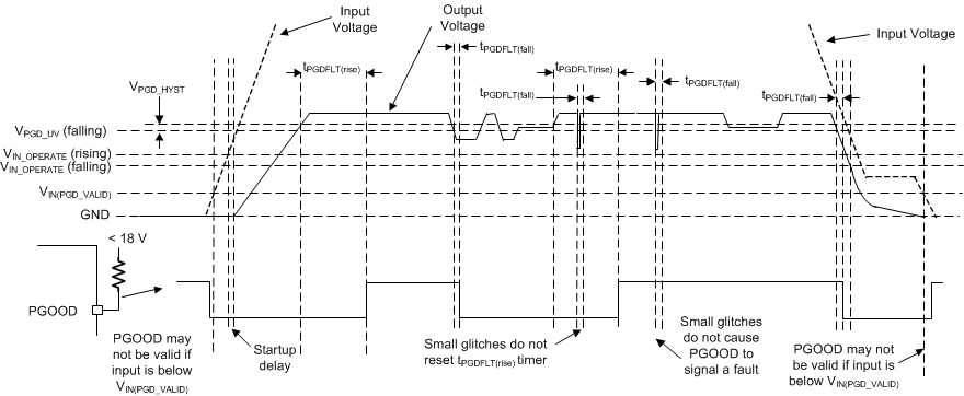
The PGOOD function is implemented to replace a discrete reset device, reducing BOM count and cost. The PGOOD pin voltage goes low when the feedback voltage is outside of the specified PGOOD thresholds (see Figure 7-7). This can occur in current limit and thermal shutdown, as well as while disabled and during normal start-up. A glitch filter prevents false flag operation for short excursions of the output voltage, such as during line and load transients. Output voltage excursions that are shorter than tPGDFLT_FALL do not trip the power-good flag. Power-good operation can be best understood by referring to Figure 8-6.
The power-good output consists of an open-drain NMOS; requiring an external pullup resistor to a suitable logic supply or VOUT. When EN is pulled low, the flag output is also forced low. With EN low, power good remains valid as long as the input voltage is ≥ 1 V (typical).
 Figure 8-6 PGOOD Timing Diagram (Excludes OV Events)
| FAULT CONDITION INITIATED | FAULT CONDITION ENDS (AFTER WHICH tPGDFLT(rise) MUST PASS BEFORE PGOOD OUTPUT IS RELEASED)(1) |
|---|---|
| VOUT < VOUT-target × PGDUV AND t > tPGDFLT(fall) | Output voltage in regulation: VOUT-target × (PGDUV + PGDHYST) < VOUT < VOUT-target × (PGDOV - PGDHYST) (See Figure 7-7.) |
| VOUT > VOUT-target × PGDOV AND t > tPGDFLT(fall) | Output voltage in regulation |
| TJ > TSD_R | TJ < TSD_F AND output voltage in regulation |
| EN < VEN falling | EN > VEN Rising AND output voltage in regulation |
| VCC < VCC_UVLO - VCC_UVLO_HYST | VCC > VCC_UVLO AND output voltage in regulation |