ZHCSMJ1 October 2021 LM61430-Q1
PRODUCTION DATA
- 1 特性
- 2 应用
- 3 说明
- 4 Revision History
- 5 Device Comparison Table
- 6 Pin Configuration and Functions
- 7 Specifications
-
8 Detailed Description
- 8.1 Overview
- 8.2 Functional Block Diagram
- 8.3
Feature Description
- 8.3.1 EN/SYNC Uses for Enable and VIN UVLO
- 8.3.2 EN/SYNC Pin Uses for Synchronization
- 8.3.3 Clock Locking
- 8.3.4 Adjustable Switching Frequency
- 8.3.5 PGOOD Output Operation
- 8.3.6 Internal LDO, VCC UVLO, and BIAS Input
- 8.3.7 Bootstrap Voltage and VCBOOT-UVLO (CBOOT Pin)
- 8.3.8 Adjustable SW Node Slew Rate
- 8.3.9 Spread Spectrum
- 8.3.10 Soft Start and Recovery From Dropout
- 8.3.11 Output Voltage Setting
- 8.3.12 Overcurrent and Short Circuit Protection
- 8.3.13 Thermal Shutdown
- 8.3.14 Input Supply Current
- 8.4 Device Functional Modes
- 9 Application and Implementation
- 10Power Supply Recommendations
- 11Layout
- 12Device and Documentation Support
- 13Mechanical, Packaging, and Orderable Information
6 Pin Configuration and Functions
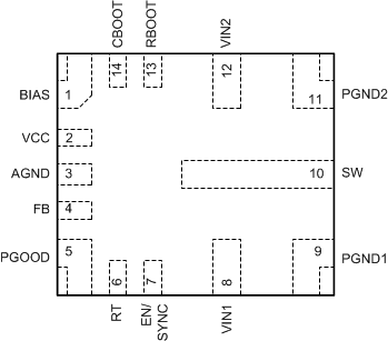
 Figure 6-1 RJR Package14-Pin VQFN-HR(Top View)
Table 6-1 Pin Functions
| PIN | I/O | DESCRIPTION | |
|---|---|---|---|
| NAME | NO. | ||
| BIAS | 1 | P | Input to internal LDO. Connect to an output voltage point to improve efficiency. Connect an optional high quality 0.1-µF to 1-µF capacitor from this pin to ground for improved noise immunity. If output voltage is above 12 V, connect this pin to ground. |
| VCC | 2 | O | Internal LDO output. Used as supply to internal control circuits. Do not connect to any external loads. Connect a high-quality 1-µF capacitor from this pin to AGND. |
| AGND | 3 | G | Analog ground for internal circuitry. Feedback and VCC are measured with respect to this pin. Must connect AGND to both PGND1 and PGND2 on the PCB. |
| FB | 4 | I | Output voltage feedback input to the internal control loop. Connect to the feedback divider tap point for adjustable output voltage. Do not float or connect to ground. |
| PGOOD | 5 | O | Open-drain power-good status output. Pull this pin up to a suitable voltage supply through a current limiting resistor. High = power OK, low = fault. PGOOD output goes low when EN = low, VIN > 1 V. |
| RT | 6 | I/O | Connect this pin to ground through a resistor with value between 5.76 kΩ and 66.5 kΩ to set switching frequency between 200 kHz and 2200 kHz. Do not float or connect to ground. |
| EN/SYNC | 7 | I | Precision enable input. High = on, Low = off. Can be connected to VIN. Precision enable allows the pin to be used as an adjustable UVLO. See Section 9. Do not float. EN/SYNC also functions as a synchronization input pin. Used to synchronize the device switching frequency to a system clock. Triggers on rising edge of external clock. A capacitor can be used to AC couple the synchronization signal to this pin. When synchronized to an external clock, the device functions in forced PWM and disables the PFM light-load efficiency mode. See Section 8. |
| VIN1 | 8 | P | Input supply to the converter. Connect a high-quality bypass capacitor or capacitors from this pin to PGND1. Low impedance connection must be provided to VIN2. |
| PGND1 | 9 | G | Power ground to the internal low-side MOSFET. Connect to system ground. Low impedance connection should be provided to PGND2. Connect a high-quality bypass capacitor or capacitors from this pin to VIN1. |
| SW | 10 | O | Switch node of the converter. Connect to the output inductor. |
| PGND2 | 11 | G | Power ground to the internal low-side MOSFET. Connect to system ground. Low impedance connection must be provided to PGND1. Connect a high-quality bypass capacitor or capacitors from this pin to VIN2. |
| VIN2 | 12 | P | Input supply to the converter. Connect a high-quality bypass capacitor or capacitors from this pin to PGND2. Low impedance connection must be provided to VIN1. |
| RBOOT | 13 | I/O | Connect to CBOOT through a resistor. This resistance must be between 0 Ω and open and determines SW node rise time. |
| CBOOT | 14 | I/O | High-side driver upper supply rail. Connect a 100-nF capacitor between SW pin and CBOOT. An internal diode connects to VCC and allows CBOOT to charge while the SW node is low. |