ZHCSMJ1 October 2021 LM61430-Q1
PRODUCTION DATA
- 1 特性
- 2 应用
- 3 说明
- 4 Revision History
- 5 Device Comparison Table
- 6 Pin Configuration and Functions
- 7 Specifications
-
8 Detailed Description
- 8.1 Overview
- 8.2 Functional Block Diagram
- 8.3
Feature Description
- 8.3.1 EN/SYNC Uses for Enable and VIN UVLO
- 8.3.2 EN/SYNC Pin Uses for Synchronization
- 8.3.3 Clock Locking
- 8.3.4 Adjustable Switching Frequency
- 8.3.5 PGOOD Output Operation
- 8.3.6 Internal LDO, VCC UVLO, and BIAS Input
- 8.3.7 Bootstrap Voltage and VCBOOT-UVLO (CBOOT Pin)
- 8.3.8 Adjustable SW Node Slew Rate
- 8.3.9 Spread Spectrum
- 8.3.10 Soft Start and Recovery From Dropout
- 8.3.11 Output Voltage Setting
- 8.3.12 Overcurrent and Short Circuit Protection
- 8.3.13 Thermal Shutdown
- 8.3.14 Input Supply Current
- 8.4 Device Functional Modes
- 9 Application and Implementation
- 10Power Supply Recommendations
- 11Layout
- 12Device and Documentation Support
- 13Mechanical, Packaging, and Orderable Information
8.4.3.3 Minimum On Time (High Input Voltage) Operation
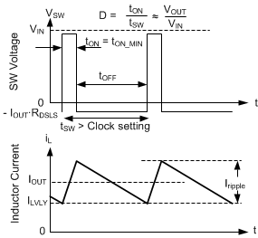
The LM61430-Q1 continues to regulate output voltage even if the input-to-output voltage ratio requires an on time less than the minimum on time of the chip with a given clock setting. This is accomplished using valley current control. At all times, the compensation circuit dictates both a maximum peak inductor current and a maximum valley inductor current. If for any reason valley current is exceeded, the clock cycle is extended until valley current falls below that determined by the compensation circuit. If the converter is not operating in current limit, the maximum valley current is set above the peak inductor current, preventing valley control from being used unless there is a failure to regulate using peak current only. If the input voltage to output voltage ratio is too high, even though current exceeds the peak value dictated by compensation, the high-side device cannot be turned off quickly enough to regulate output voltage. As a result, the compensation circuit reduces both peak and valley current. Once a low enough current is selected by the compensation circuit, valley current matches that being commanded by the compensation circuit. Under these conditions, the low-side device is kept on and the next clock cycle is prevented from starting until inductor current drops below the desired valley current. Since on-time is fixed at its minimum value, this type of operation resembles that of a device using a COT control scheme; see Figure 8-18.
