ZHCSN39A February 2020 – November 2021 LM61480 , LM61495 , LM62460
PRODUCTION DATA
- 1 特性
- 2 应用
- 3 说明
- 4 Revision History
- 5 Device Comparison Table
- 6 Pin Configuration and Functions
- 7 Specifications
-
8 Detailed Description
- 8.1 Overview
- 8.2 Functional Block Diagram
- 8.3
Feature Description
- 8.3.1 Output Voltage Selection
- 8.3.2 Enable EN Pin and Use as VIN UVLO
- 8.3.3 SYNC/MODE Uses for Synchronization
- 8.3.4 Clock Locking
- 8.3.5 Adjustable Switching Frequency
- 8.3.6 RESET Output Operation
- 8.3.7 Internal LDO, VCC UVLO, and BIAS Input
- 8.3.8 Bootstrap Voltage and VCBOOT-UVLO (CBOOT Pin)
- 8.3.9 Adjustable SW Node Slew Rate
- 8.3.10 Spread Spectrum
- 8.3.11 Soft Start and Recovery From Dropout
- 8.3.12 Overcurrent and Short Circuit Protection
- 8.3.13 Hiccup
- 8.3.14 Thermal Shutdown
- 8.4 Device Functional Modes
-
9 Application and Implementation
- 9.1 Application Information
- 9.2
Typical Application
- 9.2.1 Design Requirements
- 9.2.2
Detailed Design Procedure
- 9.2.2.1 Choosing the Switching Frequency
- 9.2.2.2 Setting the Output Voltage
- 9.2.2.3 Inductor Selection
- 9.2.2.4 Output Capacitor Selection
- 9.2.2.5 Input Capacitor Selection
- 9.2.2.6 BOOT Capacitor
- 9.2.2.7 BOOT Resistor
- 9.2.2.8 VCC
- 9.2.2.9 CFF and RFF Selection
- 9.2.2.10 RSPSP Selection
- 9.2.2.11 RT Selection
- 9.2.2.12 RMODE Selection
- 9.2.2.13 External UVLO
- 9.2.2.14 Maximum Ambient Temperature
- 9.2.3 Application Curves
- 10Power Supply Recommendations
- 11Layout
- 12Device and Documentation Support
- 13Mechanical, Packaging, and Orderable Information
8.3.9 Adjustable SW Node Slew Rate
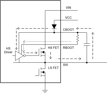
To allow optimization of EMI with respect to efficiency, the LM6x4xx is designed to allow a resistor to select the strength of the high-side FET driver during turn-on. See Figure 8-10. The current drawn through the RBOOT pin (the dotted loop) is magnified and drawn through from CBOOT (the dashed line). This current is used to turn on the high-side power MOSEFT.
 Figure 8-10 Simplified Circuit Showing How RBOOT Functions
Rise time is rapid with RBOOT short circuited to CBOOT. In this condition, SW node harmonics roll off at –20 dBµV per decade until around 150 MHz where the harmonics begin rolling off at –40 dBµV per decade. Slowing the rise time decreases the frequency where this transition occurs which provides more rolloff in the higher frequencies, which provides more margin on EMI scans. If CBOOT and RBOOT are connected through 700 Ω, slew time due to high-side turn-on is limited to no more than 13 ns. 10 ns is typical when converting 13.5 V to 5 V. This slow rise time allows energy in SW node harmonics to roll off near 50 MHz under most conditions. Rolling off harmonics eliminates the need for shielding and common mode chokes in many applications. Note that rise time increases with increasing input voltage. Noise due to stored charge is also greatly reduced with higher RBOOT resistance. Switching with a slower slew rate decreases efficiency. Take care to optimize the resistance to provide the best EMI while not generating too much heat. If RBOOT is left open, rise time is set to its maximum value.