ZHCSLY1D February 2020 – August 2021 LM61480-Q1 , LM61495-Q1 , LM62460-Q1
PRODUCTION DATA
- 1 特性
- 2 应用
- 3 说明
- 4 Revision History
- 5 Device Comparison Table
- 6 Pin Configuration and Functions
- 7 Specifications
-
8 Detailed Description
- 8.1 Overview
- 8.2 Functional Block Diagram
- 8.3
Feature Description
- 8.3.1 Output Voltage Selection
- 8.3.2 Enable EN Pin and Use as VIN UVLO
- 8.3.3 SYNC/MODE Uses for Synchronization
- 8.3.4 Clock Locking
- 8.3.5 Adjustable Switching Frequency
- 8.3.6 RESET Output Operation
- 8.3.7 Internal LDO, VCC UVLO, and BIAS Input
- 8.3.8 Bootstrap Voltage and VCBOOT-UVLO (CBOOT Pin)
- 8.3.9 Adjustable SW Node Slew Rate
- 8.3.10 Spread Spectrum
- 8.3.11 Soft Start and Recovery From Dropout
- 8.3.12 Overcurrent and Short Circuit Protection
- 8.3.13 Hiccup
- 8.3.14 Thermal Shutdown
- 8.4 Device Functional Modes
-
9 Application and Implementation
- 9.1 Application Information
- 9.2
Typical Application
- 9.2.1 Design Requirements
- 9.2.2
Detailed Design Procedure
- 9.2.2.1 Choosing the Switching Frequency
- 9.2.2.2 Setting the Output Voltage
- 9.2.2.3 Inductor Selection
- 9.2.2.4 Output Capacitor Selection
- 9.2.2.5 Input Capacitor Selection
- 9.2.2.6 BOOT Capacitor
- 9.2.2.7 BOOT Resistor
- 9.2.2.8 VCC
- 9.2.2.9 CFF and RFF Selection
- 9.2.2.10 RSPSP Selection
- 9.2.2.11 RT Selection
- 9.2.2.12 RMODE Selection
- 9.2.2.13 External UVLO
- 9.2.2.14 Maximum Ambient Temperature
- 9.2.3 Application Curves
- 10Power Supply Recommendations
- 11Layout
- 12Device and Documentation Support
- 13Mechanical, Packaging, and Orderable Information
8.3.10 Spread Spectrum
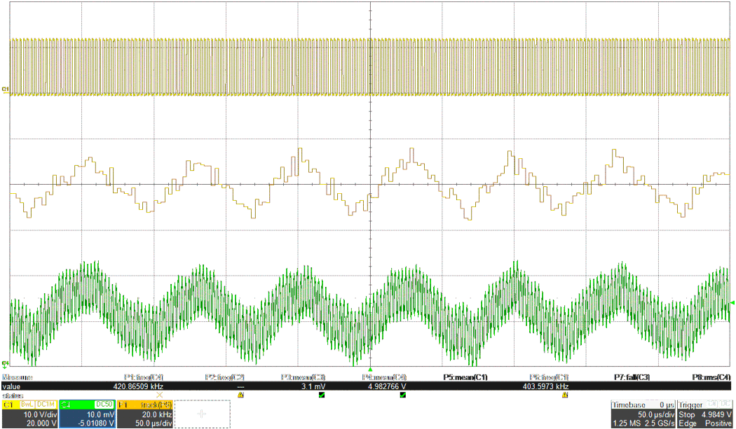
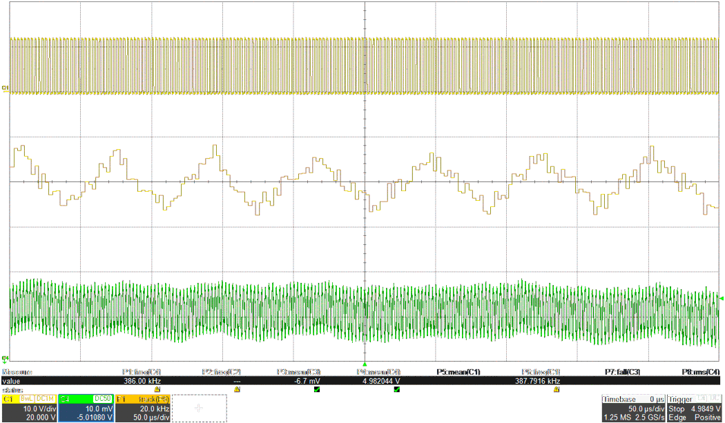
Spread spectrum is configurable using the SPSP pin. Spread spectrum eliminates peak emissions at specific frequencies by spreading these peaks across a wider range of frequencies than a part with fixed-frequency operation. The LM6x4xx-Q1 implements a modulation pattern designed to reduce low frequency-conducted emissions from the first few harmonics of the switching frequency. The pattern can also help reduce the higher harmonics that are more difficult to filter, which can fall in the FM band. These harmonics often couple to the environment through electric fields around the switch node and inductor. The LM6x4xx-Q1 uses a ±4% (typical) spread of frequencies which can spread energy smoothly across the FM and TV bands. The device implements Dual Random Spread Spectrum (DRSS). DRSS is a combination of a triangular frequency spreading pattern and pseudorandom frequency hopping. The combination allows the spread spectrum to be very effective at spreading the energy at the following:
- Fundamental switching harmonic with slow triangular pattern
- High frequency harmonics with additional psuedorandom jumps at the switching frequency

 Figure 8-11 Output Ripple Without
Ripple Cancellation Showing VSW (top), FSW (middle),
VOUT (bottom)
 Figure 8-12 Output Ripple with Ripple
Cancellation Showing VSW (top), FSW (middle),
VOUT (bottom)
Figure 8-12 Output Ripple with Ripple
Cancellation Showing VSW (top), FSW (middle),
VOUT (bottom)The spread spectrum is only available while the clock of the LM6x4xx-Q1 are free running at their natural frequency. Any of the following conditions overrides spread spectrum, turning it off:
- The clock is slowed due to operation at low input voltage. This is operation in dropout.
- The clock is slowed under light load in auto mode. This is normally not seen above 750-mA load. Note that if the device is operating in FPWM mode, spread spectrum is active, even if there is no load.
- The clock is slowed due to high input-to-output voltage ratio. This mode of operation is expected if on-time reaches minimum on-time. See the Timing Characteristics.
- The clock is synchronized with an external clock.