ZHCSL46D March 2020 – June 2021 LM62440-Q1
PRODUCTION DATA
- 1 特性
- 2 应用
- 3 说明
- 4 Revision History
- 5 Description (continued)
- 6 Device Comparison Table
- 7 Pin Configuration and Functions
- 8 Specifications
-
9 Detailed Description
- 9.1 Overview
- 9.2 Functional Block Diagram
- 9.3
Feature Description
- 9.3.1 EN Uses for Enable and VIN UVLO
- 9.3.2 MODE/SYNC Pin Operation
- 9.3.3 PGOOD Output Operation
- 9.3.4 Internal LDO, VCC UVLO, and BIAS Input
- 9.3.5 Bootstrap Voltage and VCBOOT-UVLO (CBOOT Pin)
- 9.3.6 Adjustable SW Node Slew Rate
- 9.3.7 Spread Spectrum
- 9.3.8 Soft Start and Recovery From Dropout
- 9.3.9 Output Voltage Setting
- 9.3.10 Overcurrent and Short Circuit Protection
- 9.3.11 Thermal Shutdown
- 9.3.12 Input Supply Current
- 9.4 Device Functional Modes
-
10Application and Implementation
- 10.1 Application Information
- 10.2
Typical Application
- 10.2.1 Design Requirements
- 10.2.2
Detailed Design Procedure
- 10.2.2.1 Choosing the Switching Frequency
- 10.2.2.2 Setting the Output Voltage
- 10.2.2.3 Inductor Selection
- 10.2.2.4 Output Capacitor Selection
- 10.2.2.5 Input Capacitor Selection
- 10.2.2.6 BOOT Capacitor
- 10.2.2.7 BOOT Resistor
- 10.2.2.8 VCC
- 10.2.2.9 BIAS
- 10.2.2.10 CFF and RFF Selection
- 10.2.2.11 External UVLO
- 10.2.3 Application Curves
- 11Power Supply Recommendations
- 12Layout
- 13Device and Documentation Support
- 14Mechanical, Packaging, and Orderable Information
9.3.6 Adjustable SW Node Slew Rate
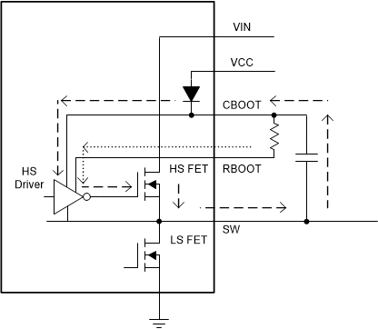
To allow optimization of EMI with respect to efficiency, the LM62440-Q1 is designed to allow a resistor to select the strength of the driver of the high-side FET during turn on. See Figure 9-14. The current drawn through the RBOOT pin (the dotted loop) is magnified and drawn through from CBOOT (the dashed line). This current is used to turn on the high-side power MOSEFT.
 Figure 9-14 Simplified Circuit Showing How RBOOT Functions
With RBOOT short circuited to CBOOT, rise time is very fast. As a result, SW node harmonics do not "roll off" until above 150 MHz. A boot resistor of 100 Ω corresponds to approximately 2.7-ns SW node rise, and this 100-Ω boot resistor virtually eliminates SW node overshoot. The slower rise time allows energy in SW node harmonics to roll off near 100 MHz under most conditions. Rolling off harmonics eliminates the need for shielding and common mode chokes in many applications. Note that rise time increases with increasing input voltage. Noise due to stored charge is also greatly reduced with higher RBOOT resistance. Switching with slower slew rate also decreases the efficiency.